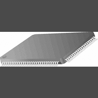
PC87393VJG National Semiconductor, PC87393VJG Datasheet - Page 37

PC87393VJG
Manufacturer Part Number
PC87393VJG
Description
IC, SUPER I/O DEVICE, TQFP-100
Manufacturer
National Semiconductor
Specifications of PC87393VJG
Data Rate
2Mbps
Supply Voltage Range
3V to 3.6V
Logic Case Style
TQFP
No. Of Pins
100
Operating Temperature Range
0°C to +70°C
Termination Type
SMD
Transceiver Type
Interface
Rohs Compliant
No
Available stocks
Company
Part Number
Manufacturer
Quantity
Price
Part Number:
PC87393VJG
Manufacturer:
NS/国半
Quantity:
20 000
2.0 Device Architecture and Configuration
LPC-FWH Address Translation: The address field in the LPC-FWH transaction is constructed of eight nibbles. The first
seven nibbles correspond to the first LS seven address nibbles (A27-A0), as follows: the first incoming nibble corresponds
to addresses A27 - A24, the second to A23 - A20, and so forth until the seventh nibble, which corresponds to A3 - A0. In-
coming nibble eight is ignored. The MS bits of the 32-bit addresses are ’1111’ (A31 - A28).
2.8.2
The PC8739x supports the CLKRUN I/O signal, whose use is highly recommended in portable systems. This signal is im-
plemented according to the specification in PCI Mobile Design Guide , Revision 1.1, December 18, 1998. The PC8739x sup-
ports operation with both a slow and stopped clock in ACPI state S0 (the system is active but is not being accessed). The
PC8739x drives the CLKRUN signal low to force the LPC bus clock into full speed operation in the following cases:
Note: When the CLKRUN signal is not in use, the PC8739x assumes valid clock on the CLKIN pin.
2.8.3
The PC8739x supports the LPCPD input. This signal is used in case the V
the LPC bus. The LPCPD signal conforms with Intel’s LPC Interface Specification , Revision 1.00. Note that if the PC8739x
power supply exists while LPCPD is active, it is not mandatory to reset the PC8739x when LPCPD is de-asserted.
2.9 REGISTER TYPE ABBREVIATIONS
The following abbreviations are used to indicate the Register Type:
2.10 SUPERI/O CONFIGURATION REGISTERS
This section describes the SuperI/O configuration and ID registers (those registers with first level indexes in the range of 20h
- 2Eh). See Table 15 for a summary and directory of these registers.
Note: Set the configuration registers to enable functions or signals that are relevant to the specific device. The val-
ues of fields that select functions, or signals, that are excluded from a specific device are treated as reserved and
should not be selected.
An IRQ is pending internally, waiting to be sent through the serial IRQ.
A DMA request or abort is pending internally, waiting to be sent through the serial DMA.
R/W = Read/Write
R = Read from a specific address returns the value of a specific register. Write to the same address is to a different
register.
W = Write
RO = Read Only
R/W1C = Read/Write 1 to Clear. Writing 1 to a bit clears it to 0. Writing 0 has no effect.
CLKRUN Functionality
LPCPD Functionality
2Bh - 2Fh
Index
20h
21h
22h
23h
24h
25h
26h
27h
28h
29h
2Ah
SID
SIOCF1
SIOCF2
SIOCF3
SIOCF4
SIOCF5
SIOCF6
SRID
SIOCF8
SIOCF9
SIOCFA
Reserved exclusively for National use
Mnemonic
SuperI/O ID
SuperI/O Configuration 1
SuperI/O Configuration 2
SuperI/O Configuration 3
SuperI/O Configuration 4
SuperI/O Configuration 5
SuperI/O Configuration 6
SuperI/O Revision ID
SuperI/O Configuration 8
SuperI/O Configuration 9
SuperI/O Configuration A
Table 15. SuperI/O Configuration Registers
Register Name
37
(Continued)
Power Well
V
V
V
V
V
V
V
V
V
V
V
DD
DD
DD
DD
DD
DD
DD
DD
DD
DD
DD
DD
chip supply is not shared by all residents of
Type
R/W
R/W
R/W
R/W
R/W
R/W
R/W
R/W
R/W
RO
RO
Section
2.10.10
2.10.11
2.10.1
2.10.2
2.10.3
2.10.4
2.10.5
2.10.6
2.10.7
2.10.8
2.10.9
www.national.com


