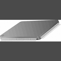
PC87393VJG National Semiconductor, PC87393VJG Datasheet - Page 73

PC87393VJG
Manufacturer Part Number
PC87393VJG
Description
IC, SUPER I/O DEVICE, TQFP-100
Manufacturer
National Semiconductor
Specifications of PC87393VJG
Data Rate
2Mbps
Supply Voltage Range
3V to 3.6V
Logic Case Style
TQFP
No. Of Pins
100
Operating Temperature Range
0°C to +70°C
Termination Type
SMD
Transceiver Type
Interface
Rohs Compliant
No
Available stocks
Company
Part Number
Manufacturer
Quantity
Price
Part Number:
PC87393VJG
Manufacturer:
NS/国半
Quantity:
20 000
- Current page: 73 of 148
- Download datasheet (703Kb)
3.0 General-Purpose Input/Output (GPIO) Port
3.2 BASIC FUNCTIONALITY
The basic functionality of each GPIO pin is based on four configuration bits and a bit slice of runtime registers GPDO and
GPDI. The configuration and operation of a single pin GPIOXn (pin n in port X) is shown in Figure 9.
3.2.1
The GPCFG register controls the following basic configuration options:
3.2.2
The value that is written to the GPDO register is driven to the pin, if the output is enabled. Reading from the GPDO register
returns its contents, regardless of the pin value or the port configuration. The GPDI register is a read-only register. Reading
from the GPDI register returns the pin value, regardless of what is driving it (the port itself, configured as an output port, or
the external device when the port is configured as an input port). Writing to this register is ignored.
Activation of the GPIO port is controlled by external device specific configuration bit (or a combination of bits). When the port
is inactive, access to GPDI and GPDO registers is disabled, and the inputs are blocked. However, there is no change in the
port configuration and in the GPDO value, and hence there is no effect on the outputs of the pins.
•
•
•
•
Port Direction - Controlled by the Output Enable bit (bit 0)
Output Type - Push-pull vs. open-drain. It is controlled by Output Buffer Type (bit 1) by enabling/disabling the pull-up
portion of the output buffer.
Weak Static Pull-Up - May be added to any type of port (input, open-drain or push-pull). It is controlled by Pull-Up Control
(bit 2).
Pin Lock - GPIO pin may be locked to prevent any changes in the output value and/or the output characteristics. The
lock is controlled by Lock (bit 3). It disables writes to the GPDO register bits, and to bits 0-3 of the GPCFG register (In-
cluding the Lock bit itself). Once locked, it can be released by hardware reset only.
Internal
Bus
Configuration Options
Operation
Read/Write
Read Only
Data In
Data Out
Lock
Bit 3
GPIO Pin Configuration (GPCFG) Register
Figure 9. GPIO Basic Functionality
Pull-Up
Control
Bit 2
Push-Pull =1
Output
Type
73
Bit 1
(Continued)
GPIO Device
Enable
Output
Enable
Bit 0
Pull-Up
Enable
Pull-Up
Static
www.national.com
Pin
Related parts for PC87393VJG
Image
Part Number
Description
Manufacturer
Datasheet
Request
R
Part Number:
Description:
National Semiconductor [8-Bit D/A Converter]
Manufacturer:
National Semiconductor
Datasheet:
Part Number:
Description:
National Semiconductor [Media Coprocessor]
Manufacturer:
National Semiconductor
Datasheet:
Part Number:
Description:
Digitally Controlled Tone and Volume Circuit with Stereo Audio Power Amplifier, Microphone Preamp Stage and National 3D Sound
Manufacturer:
National Semiconductor
Datasheet:
Part Number:
Description:
Digitally Controlled Tone and Volume Circuit with Stereo Audio Power Amplifier, Microphone Preamp Stage and National 3D Sound
Manufacturer:
National Semiconductor
Datasheet:
Part Number:
Description:
AC97 Rev 2 Codec with Sample Rate Conversion and National 3D Sound
Manufacturer:
National Semiconductor
Part Number:
Description:
Manufacturer:
National Semiconductor
Datasheet:
Part Number:
Description:
Manufacturer:
National Semiconductor
Datasheet:
Part Number:
Description:
General Purpose, Low Voltage, Low Power, Rail-to-Rail Output Operational Amplifiers
Manufacturer:
National Semiconductor
Datasheet:
Part Number:
Description:
8-bit 20 MSPS flash A/D converter.
Manufacturer:
National Semiconductor
Datasheet:
Part Number:
Description:
Low Noise Quad Operational Amplifier
Manufacturer:
National Semiconductor
Datasheet:
Part Number:
Description:
Quad Differential Line Receivers
Manufacturer:
National Semiconductor
Datasheet:
Part Number:
Description:
Quad High Speed Trapezoidal? Bus Transceiver
Manufacturer:
National Semiconductor
Datasheet:
Part Number:
Description:
Dual Line Receiver
Manufacturer:
National Semiconductor
Datasheet:
Part Number:
Description:
TTL to 10k ECL Level Translator with Latch
Manufacturer:
National Semiconductor
Datasheet:


