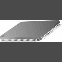
PC87393VJG National Semiconductor, PC87393VJG Datasheet - Page 131

PC87393VJG
Manufacturer Part Number
PC87393VJG
Description
IC, SUPER I/O DEVICE, TQFP-100
Manufacturer
National Semiconductor
Specifications of PC87393VJG
Data Rate
2Mbps
Supply Voltage Range
3V to 3.6V
Logic Case Style
TQFP
No. Of Pins
100
Operating Temperature Range
0°C to +70°C
Termination Type
SMD
Transceiver Type
Interface
Rohs Compliant
No
Available stocks
Company
Part Number
Manufacturer
Quantity
Price
Part Number:
PC87393VJG
Manufacturer:
NS/国半
Quantity:
20 000
- Current page: 131 of 148
- Download datasheet (703Kb)
8.0 Legacy Functional Blocks
8.4 IR FUNCTIONALITY (SP2)
8.4.1
This section describes the IR support registers of Serial Port 2 (SP2). The UART support registers for both SP1 and SP2
are described in Section 8.3.
The IR functional block provides advanced, versatile serial communications features with IR capabilities.
SP2 supports also two DMA channels; the functional block can use either one or both of them. One channel is required for
IR-based applications, since IR communication works in half duplex fashion. Two channels would normally be needed to
handle high-speed full duplex UART based applications.
8.4.2
Eight register banks, each containing eight registers, control SP2 operation. Banks 0-3 are used to control both UART and
IR modes of operation; banks 4-7 are used to control and configure the IR modes of operation only. All registers use the
same 8-byte address space to indicate offsets 00h through 07h. The BSR register selects the active bank and is common
to all banks. See Figure 31.
General Description
IR Mode Register Bank Overview
Offset 07h
Offset 06h
Offset 05h
Offset 04h
Offset 02h
Offset 01h
Offset 00h
LCR/BSR
BANK 0
BANK 1
BANK 2
Figure 31. SP2 Register Bank Architecture
BANK 3
(Continued)
BANK 4
BANK 5
BANK 6
BANK 7
131
IR Special Banks
(Banks 4-7)
Common
Register
Throughout
All Banks
www.national.com
Related parts for PC87393VJG
Image
Part Number
Description
Manufacturer
Datasheet
Request
R
Part Number:
Description:
National Semiconductor [8-Bit D/A Converter]
Manufacturer:
National Semiconductor
Datasheet:
Part Number:
Description:
National Semiconductor [Media Coprocessor]
Manufacturer:
National Semiconductor
Datasheet:
Part Number:
Description:
Digitally Controlled Tone and Volume Circuit with Stereo Audio Power Amplifier, Microphone Preamp Stage and National 3D Sound
Manufacturer:
National Semiconductor
Datasheet:
Part Number:
Description:
Digitally Controlled Tone and Volume Circuit with Stereo Audio Power Amplifier, Microphone Preamp Stage and National 3D Sound
Manufacturer:
National Semiconductor
Datasheet:
Part Number:
Description:
AC97 Rev 2 Codec with Sample Rate Conversion and National 3D Sound
Manufacturer:
National Semiconductor
Part Number:
Description:
Manufacturer:
National Semiconductor
Datasheet:
Part Number:
Description:
Manufacturer:
National Semiconductor
Datasheet:
Part Number:
Description:
General Purpose, Low Voltage, Low Power, Rail-to-Rail Output Operational Amplifiers
Manufacturer:
National Semiconductor
Datasheet:
Part Number:
Description:
8-bit 20 MSPS flash A/D converter.
Manufacturer:
National Semiconductor
Datasheet:
Part Number:
Description:
Low Noise Quad Operational Amplifier
Manufacturer:
National Semiconductor
Datasheet:
Part Number:
Description:
Quad Differential Line Receivers
Manufacturer:
National Semiconductor
Datasheet:
Part Number:
Description:
Quad High Speed Trapezoidal? Bus Transceiver
Manufacturer:
National Semiconductor
Datasheet:
Part Number:
Description:
Dual Line Receiver
Manufacturer:
National Semiconductor
Datasheet:
Part Number:
Description:
TTL to 10k ECL Level Translator with Latch
Manufacturer:
National Semiconductor
Datasheet:


