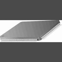
PC87393VJG National Semiconductor, PC87393VJG Datasheet - Page 33

PC87393VJG
Manufacturer Part Number
PC87393VJG
Description
IC, SUPER I/O DEVICE, TQFP-100
Manufacturer
National Semiconductor
Specifications of PC87393VJG
Data Rate
2Mbps
Supply Voltage Range
3V to 3.6V
Logic Case Style
TQFP
No. Of Pins
100
Operating Temperature Range
0°C to +70°C
Termination Type
SMD
Transceiver Type
Interface
Rohs Compliant
No
Available stocks
Company
Part Number
Manufacturer
Quantity
Price
Part Number:
PC87393VJG
Manufacturer:
NS/国半
Quantity:
20 000
2.0 Device Architecture and Configuration
2.3 THE CLOCK MULTIPLIER
The source of all internal clocks in the chip is either an external 48 MHz clock on the CLKIN pin, or the on-chip clock multi-
plier. The clock multiplier is fed by applying a clock source at one of two frequencies on the CLKIN pin: 32.768 KHz or
14.31818 MHz. The clock multiplier generates two internal clocks, 24 MHz and 48 MHz. These clocks are needed for all the
modules in the PC8739x with the exception of the X-Bus module. After power-up or reset, the clock (clock multiplier or ex-
ternal clock) is disabled.
2.3.1
The on-chip clock multiplier starts working when it is enabled by bit 2 of the SIOCF9 register, index 29h, i.e., when its value
changes from 0 to 1 (only for source clocks 32.768 KHz or 14.31818 MHz). This bit can also disable the clock multiplier and
its output clock after the multiplier is enabled. Once enabled, the output clock is frozen to a steady logic level until the mul-
tiplier provides a stable output clock that meets all requirements. Then the clock starts toggling.
On power-up when V
of the clock multiplier may toggle regardless of the state of the Master Reset (MR) pin. The clock multiplier waits for a toggling
input clock.
Bit 3 of the SIOCF9 register, a read only bit, is the Valid Clock Multiplier status bit. While stabilizing, the output clock is frozen
to a steady logic level, and the status bit is cleared to 0 to indicate a frozen clock. When the clock multiplier is stable, the
output clock starts toggling and the status bit is set to 1. It tells the software when the clock multiplier is ready. The software
should poll this status bit until it is set (1), and only then activate (enable) the FDC, Parallel Port, UARTs and infrared inter-
face. When the multiplier is enabled for the first time after power-up, more time is required until this status bit is set to 1.
The clock multiplier and its output clock do not consume power when they are disabled.
2.3.2
To ensure proper operation, proceed as follows after power-up:
1. Set bits 2, 1 and 0 of the Clock Control Configuration register (SIOCF9) at index 29h according to the clock source used
2. Enable the clock.
If the clock source is 32.768 kHz or 14.31818 MHz:
3. Enable any module in the chip, as needed.
2.3.3
Before disabling the clock multiplier (by clearing bit 2 of SIOCF9 Register) or the external clock (for 48 MHz), make sure that
all PC8739x modules are disabled. This is done by polling bit 4 of the SIOCF9 register (Module Enable Status) for 0.
2.3.4
Wake-up time is 33 msec (maximum). This is measured from valid V
until the clock is stable. Tolerance (long term deviation) of the multiplier output clock, relative to the input clock, is 110 ppm.
Total tolerance is therefore
(even if the external clock is the default frequency setting). See Table 13. Bits 2, 1 and 0 may be written in a single write
cycle. From this point on, bits 1 and 0 of the SIOCF9 register are read only. The value of the clock source cannot be
changed, except by a total power-down and power-up cycle. However, the clock can be disabled at any time.
— Poll bit 3 of the SIOCF9 register while the clock multiplier is stabilizing.
— When bit 3 of SIOCF9 is set to 1, go to step 3.
Functionality
Chip Power-Up
Disabling the Clock
Specifications
External Source on CLKIN Pin
14.31818 MHz clock multiplier
32.768 KHz clock multiplier
External 48 MHz clock
DD
is applied, the chip wakes up with the on-chip clock multiplier disabled. The input and output clocks
No clock
(input clock tolerance + 110 ppm). Cycle by cycle variance is 0.4 nsec (maximum).
Table 13. Clock Multiplier Encoding Options
Valid Clock
0 = Frozen
1 = Stable
Multiplier
Always 1
Status
Bit 3
0
33
(Continued)
SIOCF9 Register (Index 29h)
DD
Clock Enable
toggling of the input clock and multiplier enabled
Bit 2
1
1
1
0
Chip Clock
Bit 1 Bit 0
10, 01, 00
0
0
1
Source
0
1
0
www.national.com


