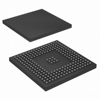
AT91SAM9RL64-CU Atmel, AT91SAM9RL64-CU Datasheet - Page 260

AT91SAM9RL64-CU
Manufacturer Part Number
AT91SAM9RL64-CU
Description
IC ARM9 MCU 217-LFBGA
Manufacturer
Atmel
Series
AT91SAMr
Specifications of AT91SAM9RL64-CU
Core Processor
ARM9
Core Size
16/32-Bit
Speed
240MHz
Connectivity
EBI/EMI, I²C, MMC, SPI, SSC, UART/USART, USB
Peripherals
AC'97, LCD, POR, PWM, WDT
Number Of I /o
118
Program Memory Size
32KB (32K x 8)
Program Memory Type
ROM
Ram Size
72K x 8
Voltage - Supply (vcc/vdd)
1.08 V ~ 1.32 V
Data Converters
A/D 6x10b
Oscillator Type
Internal
Operating Temperature
-40°C ~ 85°C
Package / Case
217-LFBGA
Processor Series
AT91SAMx
Core
ARM926EJ-S
Data Bus Width
32 bit
Data Ram Size
64 KB
Interface Type
2-Wire, SPI, SSC, USART
Maximum Clock Frequency
240 MHz
Number Of Programmable I/os
118
Number Of Timers
4
Maximum Operating Temperature
+ 85 C
Mounting Style
SMD/SMT
3rd Party Development Tools
JTRACE-ARM-2M, MDK-ARM, RL-ARM, ULINK2
Development Tools By Supplier
AT91SAM-ICE, AT91-ISP
Minimum Operating Temperature
- 40 C
On-chip Adc
10 bit, 6 Channel
Controller Family/series
AT91SAM9xxx
No. Of I/o's
118
Ram Memory Size
64KB
Cpu Speed
240MHz
No. Of Timers
1
Rohs Compliant
Yes
Package
217LFBGA
Device Core
ARM926EJ-S
Family Name
91S
Maximum Speed
240 MHz
Operating Supply Voltage
1.8|3.3 V
For Use With
AT91SAM9RL-EK - KIT EVAL FOR AT91SAM9RLAT91SAM-ICE - EMULATOR FOR AT91 ARM7/ARM9
Lead Free Status / RoHS Status
Lead free / RoHS Compliant
Eeprom Size
-
Lead Free Status / Rohs Status
Lead free / RoHS Compliant
Available stocks
Company
Part Number
Manufacturer
Quantity
Price
Company:
Part Number:
AT91SAM9RL64-CU
Manufacturer:
ATMEL
Quantity:
16
Company:
Part Number:
AT91SAM9RL64-CU
Manufacturer:
ATMEL
Quantity:
255
Part Number:
AT91SAM9RL64-CU
Manufacturer:
ATMEGL
Quantity:
20 000
- Current page: 260 of 903
- Download datasheet (13Mb)
26.6.2
26.6.3
260
AT91SAM9R64/RL64 Preliminary
Divider and Phase Lock Loop Programming
UTMI Bias and Phase Lock Loop Programming
Figure 26-6. PLL Capacitors and Resistors
Values of R, C1 and C2 to be connected to the PLLRC pin must be calculated as a function of
the PLL input frequency, the PLL output frequency and the phase margin. A trade-off has to be
found between output signal overshoot and startup time.
The divider can be set between 1 and 255 in steps of 1. When a divider field (DIV) is set to 0, the
output of the corresponding divider and the PLL output is a continuous signal at level 0. On
reset, each DIV field is set to 0, thus the corresponding PLL input clock is set to 0.
The PLL allows multiplication of the divider’s outputs. The PLL clock signal has a frequency that
depends on the respective source signal frequency and on the parameters DIV and MUL. The
factor applied to the source signal frequency is (MUL + 1)/DIV. When MUL is written to 0, the
corresponding PLL is disabled and its power consumption is saved. Re-enabling the PLL can be
performed by writing a value higher than 0 in the MUL field.
Whenever the PLL is re-enabled or one of its parameters is changed, the LOCK bit in PMC_SR
is automatically cleared. The values written in the PLLCOUNT field in CKGR_PLLR are loaded
in the PLL counter. The PLL counter then decrements at the speed of the Slow Clock until it
reaches 0. At this time, the LOCK bit is set in PMC_SR and can trigger an interrupt to the pro-
cessor. The user has to load the number of Slow Clock cycles required to cover the PLL
transient time into the PLLCOUNT field. The transient time depends on the PLL filter. The initial
state of the PLL and its target frequency can be calculated using a specific tool provided by
Atmel.
The multiplier is hard-wired to 40 to obtain the USB High Speed 480 MHz.
MAINCK
SLCK
C2
C1
R
PLLCOUNT
PLLRC
UPLLEN
Counter
PLL
PLL
GND
PLL
LOCKU
USBHSCK
6289C–ATARM–28-May-09
Related parts for AT91SAM9RL64-CU
Image
Part Number
Description
Manufacturer
Datasheet
Request
R

Part Number:
Description:
MCU, MPU & DSP Development Tools KICKSTART KIT FOR AT91SAM9 PLUS
Manufacturer:
IAR Systems

Part Number:
Description:
DEV KIT FOR AVR/AVR32
Manufacturer:
Atmel
Datasheet:

Part Number:
Description:
INTERVAL AND WIPE/WASH WIPER CONTROL IC WITH DELAY
Manufacturer:
ATMEL Corporation
Datasheet:

Part Number:
Description:
Low-Voltage Voice-Switched IC for Hands-Free Operation
Manufacturer:
ATMEL Corporation
Datasheet:

Part Number:
Description:
MONOLITHIC INTEGRATED FEATUREPHONE CIRCUIT
Manufacturer:
ATMEL Corporation
Datasheet:

Part Number:
Description:
AM-FM Receiver IC U4255BM-M
Manufacturer:
ATMEL Corporation
Datasheet:

Part Number:
Description:
Monolithic Integrated Feature Phone Circuit
Manufacturer:
ATMEL Corporation
Datasheet:

Part Number:
Description:
Multistandard Video-IF and Quasi Parallel Sound Processing
Manufacturer:
ATMEL Corporation
Datasheet:

Part Number:
Description:
High-performance EE PLD
Manufacturer:
ATMEL Corporation
Datasheet:

Part Number:
Description:
8-bit Flash Microcontroller
Manufacturer:
ATMEL Corporation
Datasheet:

Part Number:
Description:
2-Wire Serial EEPROM
Manufacturer:
ATMEL Corporation
Datasheet:


