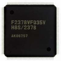
DF61657CN35FTV Renesas Electronics America, DF61657CN35FTV Datasheet - Page 166

DF61657CN35FTV
Manufacturer Part Number
DF61657CN35FTV
Description
IC H8SX/1657 MCU FLASH 120TQFP
Manufacturer
Renesas Electronics America
Series
H8® H8SX/1600r
Datasheet
1.DF61656N35FTV.pdf
(894 pages)
Specifications of DF61657CN35FTV
Core Processor
H8SX
Core Size
32-Bit
Speed
35MHz
Connectivity
SCI, SmartCard
Peripherals
DMA, PWM, WDT
Number Of I /o
82
Program Memory Size
768KB (768K x 8)
Program Memory Type
FLASH
Ram Size
24K x 8
Voltage - Supply (vcc/vdd)
3 V ~ 3.6 V
Data Converters
A/D 8x10b; D/A 2x8b
Oscillator Type
Internal
Operating Temperature
-20°C ~ 75°C
Package / Case
120-TQFP, 120-VQFP
For Use With
3DK1657 - DEV EVAL KIT FOR H8SX/1657
Lead Free Status / RoHS Status
Lead free / RoHS Compliant
Eeprom Size
-
Available stocks
Company
Part Number
Manufacturer
Quantity
Price
Company:
Part Number:
DF61657CN35FTV
Manufacturer:
RENESAS
Quantity:
101
Company:
Part Number:
DF61657CN35FTV
Manufacturer:
Renesas Electronics America
Quantity:
10 000
- Current page: 166 of 894
- Download datasheet (5Mb)
Section 6 Bus Controller (BSC)
6.2.4
RDNCR selects the negation timing of the read strobe signal (RD) when reading the external
address spaces specified as a basic bus interface or the address/data multiplexed I/O interface.
Notes: 1. In an external address space which is specified as byte control SRAM interface, the
Rev. 2.00 Jun. 28, 2007 Page 140 of 864
REJ09B0341-0200
Bit
15
14
13
12
11
10
9
8
7 to 0
Bit
Bit Name
Initial Value
R/W
Bit
Bit Name
Initial Value
R/W
2. In an external address space which is specified as burst ROM interface, the RDNCR
Bit Name
RDN7
RDN6
RDN5
RDN4
RDN3
RDN2
RDN1
RDN0
Read Strobe Timing Control Register (RDNCR)
RDNCR setting is ignored and the same operation when RDNn = 1 is performed.
setting is ignored during CPU read accesses and the same operation when RDNn = 0 is
performed.
RDN7
R/W
15
R
0
7
0
Initial
Value
0
0
0
0
0
0
0
0
All 0
RDN6
R/W
14
R
0
6
0
R/W
R/W
R/W
R/W
R/W
R/W
R/W
R/W
R/W
R
RDN5
R/W
13
R
0
5
0
Description
Read Strobe Timing Control
These bits set the negation timing of the read strobe in a
corresponding area read access.
As shown in figure 6.2, the read strobe for an area for
which the RDNn bit is set to 1 is negated one half-cycle
earlier than that for an area for which the RDNn bit is
cleared to 0. The read data setup and hold time are also
given one half-cycle earlier.
0: In an area n read access, the RD signal is negated at
1: In an area n read access, the RD signal is negated one
(n = 7 to 0)
Reserved
These are read-only bits and cannot be modified.
the end of the read cycle
half-cycle before the end of the read cycle
RDN4
R/W
12
R
0
4
0
RDN3
R/W
11
R
0
3
0
RDN2
R/W
10
R
0
2
0
RDN1
R/W
R
9
0
1
0
RDN0
R/W
R
8
0
0
0
Related parts for DF61657CN35FTV
Image
Part Number
Description
Manufacturer
Datasheet
Request
R

Part Number:
Description:
KIT STARTER FOR M16C/29
Manufacturer:
Renesas Electronics America
Datasheet:

Part Number:
Description:
KIT STARTER FOR R8C/2D
Manufacturer:
Renesas Electronics America
Datasheet:

Part Number:
Description:
R0K33062P STARTER KIT
Manufacturer:
Renesas Electronics America
Datasheet:

Part Number:
Description:
KIT STARTER FOR R8C/23 E8A
Manufacturer:
Renesas Electronics America
Datasheet:

Part Number:
Description:
KIT STARTER FOR R8C/25
Manufacturer:
Renesas Electronics America
Datasheet:

Part Number:
Description:
KIT STARTER H8S2456 SHARPE DSPLY
Manufacturer:
Renesas Electronics America
Datasheet:

Part Number:
Description:
KIT STARTER FOR R8C38C
Manufacturer:
Renesas Electronics America
Datasheet:

Part Number:
Description:
KIT STARTER FOR R8C35C
Manufacturer:
Renesas Electronics America
Datasheet:

Part Number:
Description:
KIT STARTER FOR R8CL3AC+LCD APPS
Manufacturer:
Renesas Electronics America
Datasheet:

Part Number:
Description:
KIT STARTER FOR RX610
Manufacturer:
Renesas Electronics America
Datasheet:

Part Number:
Description:
KIT STARTER FOR R32C/118
Manufacturer:
Renesas Electronics America
Datasheet:

Part Number:
Description:
KIT DEV RSK-R8C/26-29
Manufacturer:
Renesas Electronics America
Datasheet:

Part Number:
Description:
KIT STARTER FOR SH7124
Manufacturer:
Renesas Electronics America
Datasheet:

Part Number:
Description:
KIT STARTER FOR H8SX/1622
Manufacturer:
Renesas Electronics America
Datasheet:

Part Number:
Description:
KIT DEV FOR SH7203
Manufacturer:
Renesas Electronics America
Datasheet:


