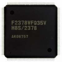
DF61657CN35FTV Renesas Electronics America, DF61657CN35FTV Datasheet - Page 771

DF61657CN35FTV
Manufacturer Part Number
DF61657CN35FTV
Description
IC H8SX/1657 MCU FLASH 120TQFP
Manufacturer
Renesas Electronics America
Series
H8® H8SX/1600r
Datasheet
1.DF61656N35FTV.pdf
(894 pages)
Specifications of DF61657CN35FTV
Core Processor
H8SX
Core Size
32-Bit
Speed
35MHz
Connectivity
SCI, SmartCard
Peripherals
DMA, PWM, WDT
Number Of I /o
82
Program Memory Size
768KB (768K x 8)
Program Memory Type
FLASH
Ram Size
24K x 8
Voltage - Supply (vcc/vdd)
3 V ~ 3.6 V
Data Converters
A/D 8x10b; D/A 2x8b
Oscillator Type
Internal
Operating Temperature
-20°C ~ 75°C
Package / Case
120-TQFP, 120-VQFP
For Use With
3DK1657 - DEV EVAL KIT FOR H8SX/1657
Lead Free Status / RoHS Status
Lead free / RoHS Compliant
Eeprom Size
-
Available stocks
Company
Part Number
Manufacturer
Quantity
Price
Company:
Part Number:
DF61657CN35FTV
Manufacturer:
RENESAS
Quantity:
101
Company:
Part Number:
DF61657CN35FTV
Manufacturer:
Renesas Electronics America
Quantity:
10 000
- Current page: 771 of 894
- Download datasheet (5Mb)
This LSI has an on-chip clock pulse generator (CPG) that generates the system clock (Iφ),
peripheral module clock (Pφ), and external bus clock (Bφ).
The clock pulse generator consists of an oscillator, a PLL (Phase Locked Loop) circuit, a divider,
and selecters. Figure 19.1 shows a block diagram of the clock pulse generat2or.
Clock frequencies can be changed by the PLL circuit and divider in the CPG. Changing the
system clock control register (SCKCR) setting by software can change the clock frequencies.
This LSI supports three types of clocks: a system clock provided to the CPU and bus masters, a
peripheral module clock provided to the peripheral modules, and an external bus clock provided to
the external bus. These clocks can be specified independently. Note, however, that the frequencies
of the peripheral clock and external bus clock are lower than that of the system clock.
EXTAL
XTAL
Oscillator
Figure 19.1 Block Diagram of Clock Pulse Generator
Section 19 Clock Pulse Generator
circuit
PLL
EXTAL × 4
and 1/8)
Divider
(1/1,
1/2,
1/4,
1/1
1/2
1/4
1/8
1/1
1/2
1/4
1/8
1/1
1/2
1/4
1/8
Rev. 2.00 Jun. 28, 2007 Page 745 of 864
Selector
Selector
Selector
SCKCR
SCKCR
SCKCR
Section 19 Clock Pulse Generator
ICK2 to ICK0
PCK2 to PCK0
BCK2 to BCK0
System clock (Iφ)
(to the CPU and
Peripheral module
clock (Pφ)
(to peripheral modules)
External bus clock (Bφ)
(to the Bφ pin)
bus masters)
REJ09B0341-0200
Related parts for DF61657CN35FTV
Image
Part Number
Description
Manufacturer
Datasheet
Request
R

Part Number:
Description:
KIT STARTER FOR M16C/29
Manufacturer:
Renesas Electronics America
Datasheet:

Part Number:
Description:
KIT STARTER FOR R8C/2D
Manufacturer:
Renesas Electronics America
Datasheet:

Part Number:
Description:
R0K33062P STARTER KIT
Manufacturer:
Renesas Electronics America
Datasheet:

Part Number:
Description:
KIT STARTER FOR R8C/23 E8A
Manufacturer:
Renesas Electronics America
Datasheet:

Part Number:
Description:
KIT STARTER FOR R8C/25
Manufacturer:
Renesas Electronics America
Datasheet:

Part Number:
Description:
KIT STARTER H8S2456 SHARPE DSPLY
Manufacturer:
Renesas Electronics America
Datasheet:

Part Number:
Description:
KIT STARTER FOR R8C38C
Manufacturer:
Renesas Electronics America
Datasheet:

Part Number:
Description:
KIT STARTER FOR R8C35C
Manufacturer:
Renesas Electronics America
Datasheet:

Part Number:
Description:
KIT STARTER FOR R8CL3AC+LCD APPS
Manufacturer:
Renesas Electronics America
Datasheet:

Part Number:
Description:
KIT STARTER FOR RX610
Manufacturer:
Renesas Electronics America
Datasheet:

Part Number:
Description:
KIT STARTER FOR R32C/118
Manufacturer:
Renesas Electronics America
Datasheet:

Part Number:
Description:
KIT DEV RSK-R8C/26-29
Manufacturer:
Renesas Electronics America
Datasheet:

Part Number:
Description:
KIT STARTER FOR SH7124
Manufacturer:
Renesas Electronics America
Datasheet:

Part Number:
Description:
KIT STARTER FOR H8SX/1622
Manufacturer:
Renesas Electronics America
Datasheet:

Part Number:
Description:
KIT DEV FOR SH7203
Manufacturer:
Renesas Electronics America
Datasheet:


