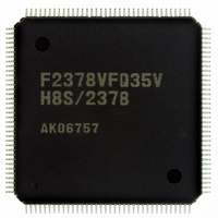
DF61657CN35FTV Renesas Electronics America, DF61657CN35FTV Datasheet - Page 9

DF61657CN35FTV
Manufacturer Part Number
DF61657CN35FTV
Description
IC H8SX/1657 MCU FLASH 120TQFP
Manufacturer
Renesas Electronics America
Series
H8® H8SX/1600r
Datasheet
1.DF61656N35FTV.pdf
(894 pages)
Specifications of DF61657CN35FTV
Core Processor
H8SX
Core Size
32-Bit
Speed
35MHz
Connectivity
SCI, SmartCard
Peripherals
DMA, PWM, WDT
Number Of I /o
82
Program Memory Size
768KB (768K x 8)
Program Memory Type
FLASH
Ram Size
24K x 8
Voltage - Supply (vcc/vdd)
3 V ~ 3.6 V
Data Converters
A/D 8x10b; D/A 2x8b
Oscillator Type
Internal
Operating Temperature
-20°C ~ 75°C
Package / Case
120-TQFP, 120-VQFP
For Use With
3DK1657 - DEV EVAL KIT FOR H8SX/1657
Lead Free Status / RoHS Status
Lead free / RoHS Compliant
Eeprom Size
-
Available stocks
Company
Part Number
Manufacturer
Quantity
Price
Company:
Part Number:
DF61657CN35FTV
Manufacturer:
RENESAS
Quantity:
101
Company:
Part Number:
DF61657CN35FTV
Manufacturer:
Renesas Electronics America
Quantity:
10 000
- Current page: 9 of 894
- Download datasheet (5Mb)
3. Description of Registers
Each register description includes a bit chart, illustrating the arrangement of bits, and a table of
bits, describing the meanings of the bit settings. The standard format and notation for bit charts
and tables are described below.
[Bit Chart]
[Table of Bits]
Initial value:
R/W:
Bit:
Note: The bit names and sentences in the above figure are examples, and have nothing to do with the contents of this
(1) Bit
(2) Bit name
(3) Initial value
(4) R/W
(5) Description
Bit
15
14
13 to 11
10
9
R/W
(1)
15
0
Indicates the bit number or numbers.
In the case of a 32-bit register, the bits are arranged in order from 31 to 0. In the case
of a 16-bit register, the bits are arranged in order from 15 to 0.
Indicates the name of the bit or bit field.
When the number of bits has to be clearly indicated in the field, appropriate notation is
included (e.g., ASID[3:0]).
A reserved bit is indicated by "−".
Certain kinds of bits, such as those of timer counters, are not assigned bit names. In such
cases, the entry under Bit Name is blank.
Indicates the value of each bit immediately after a power-on reset, i.e., the initial value.
0: The initial value is 0
1: The initial value is 1
−: The initial value is undefined
For each bit and bit field, this entry indicates whether the bit or field is readable or writable,
or both writing to and reading from the bit or field are impossible.
The notation is as follows:
R/W:
R/(W):
R:
W:
Describes the function of the bit or field and specifies the values for writing.
manual.
R/W
14
0
The bit or field is readable and writable.
The bit or field is readable and writable.
However, writing is only performed to flag clearing.
The bit or field is readable.
"R" is indicated for all reserved bits. When writing to the register, write
the value under Initial Value in the bit chart to reserved bits or fields.
The bit or field is writable.
Bit Name
−
−
ASID2 to
ASID0
−
−
−
ASID2
R/W
(2)
13
0
ASID1 ASID0
R/W
12
0
(3)
Initial Value R/W
0
0
All 0
0
1
0
R/W
11
0
10
R
0
(4)
R
R/W
R
R
R
R
9
1
Description
Reserved
These bits are always read as 0.
Address Identifier
These bits enable or disable the pin function.
Reserved
This bit is always read as 0.
Reserved
This bit is always read as 1.
R/W
8
0
R/W
7
0
R/W
6
0
R/W
Rev. 2.00 Jun. 28, 2007 Page vii of xxiv
5
0
(5)
R/W
Q
4
0
ACMP2
R/W
3
0
ACMP1 ACMP0
R/W
2
0
R/W
1
0
R/W
IFE
0
0
Related parts for DF61657CN35FTV
Image
Part Number
Description
Manufacturer
Datasheet
Request
R

Part Number:
Description:
KIT STARTER FOR M16C/29
Manufacturer:
Renesas Electronics America
Datasheet:

Part Number:
Description:
KIT STARTER FOR R8C/2D
Manufacturer:
Renesas Electronics America
Datasheet:

Part Number:
Description:
R0K33062P STARTER KIT
Manufacturer:
Renesas Electronics America
Datasheet:

Part Number:
Description:
KIT STARTER FOR R8C/23 E8A
Manufacturer:
Renesas Electronics America
Datasheet:

Part Number:
Description:
KIT STARTER FOR R8C/25
Manufacturer:
Renesas Electronics America
Datasheet:

Part Number:
Description:
KIT STARTER H8S2456 SHARPE DSPLY
Manufacturer:
Renesas Electronics America
Datasheet:

Part Number:
Description:
KIT STARTER FOR R8C38C
Manufacturer:
Renesas Electronics America
Datasheet:

Part Number:
Description:
KIT STARTER FOR R8C35C
Manufacturer:
Renesas Electronics America
Datasheet:

Part Number:
Description:
KIT STARTER FOR R8CL3AC+LCD APPS
Manufacturer:
Renesas Electronics America
Datasheet:

Part Number:
Description:
KIT STARTER FOR RX610
Manufacturer:
Renesas Electronics America
Datasheet:

Part Number:
Description:
KIT STARTER FOR R32C/118
Manufacturer:
Renesas Electronics America
Datasheet:

Part Number:
Description:
KIT DEV RSK-R8C/26-29
Manufacturer:
Renesas Electronics America
Datasheet:

Part Number:
Description:
KIT STARTER FOR SH7124
Manufacturer:
Renesas Electronics America
Datasheet:

Part Number:
Description:
KIT STARTER FOR H8SX/1622
Manufacturer:
Renesas Electronics America
Datasheet:

Part Number:
Description:
KIT DEV FOR SH7203
Manufacturer:
Renesas Electronics America
Datasheet:


