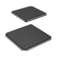
HD6417705F133BV Renesas Electronics America, HD6417705F133BV Datasheet - Page 204

HD6417705F133BV
Manufacturer Part Number
HD6417705F133BV
Description
MPU 3V 0K PB-FREE 208 FP
Manufacturer
Renesas Electronics America
Series
SuperH® SH7700r
Datasheet
1.HD6417705F133BV.pdf
(741 pages)
Specifications of HD6417705F133BV
Core Processor
SH-3
Core Size
32-Bit
Speed
133MHz
Connectivity
EBI/EMI, FIFO, IrDA, SCI, USB
Peripherals
DMA, POR, PWM, WDT
Number Of I /o
105
Program Memory Type
ROMless
Ram Size
32K x 8
Voltage - Supply (vcc/vdd)
1.4 V ~ 1.6 V
Data Converters
A/D 4x10b
Oscillator Type
Internal
Operating Temperature
-20°C ~ 75°C
Package / Case
208-LQFP
Lead Free Status / RoHS Status
Lead free / RoHS Compliant
Eeprom Size
-
Program Memory Size
-
- Current page: 204 of 741
- Download datasheet (5Mb)
Notes: 1. This register only accepts 32-bit writing to prevent incorrect writing. In this case, the
7.4.1
CMNCR is a 32-bit register that controls the common items for each area. Do not access external
memory other than area 0 until the CMNCR register initialization is complete.
Bit
31 to 8
7
6
Rev. 2.00, 09/03, page 156 of 690
Wait control register for CS6B space (CS6BWCR)
SDRAM control register (SDCR)
Refresh timer control/status register (RTCSR) *
Refresh timer counter (RTCNT) *
Refresh time constant register (RTCOR) *
SDRAM mode register for CS2 space (SDMR2) *
SDRAM mode register for CS3 space (SDMR3) *
2. The contents of this register are stored in SDRAM. When this register space is
Bit
Name
DMAIW1
DMAIW0
Common Control Register (CMNCR)
upper 16 bits of the data must be H'A55A, otherwise writing cannot be performed.
When reading, the upper 16 bits are read as H'0000.
accessed, the corresponding register in SDRAM is written to. For details, refer to
section 7.8.10, Power-On Sequence.
Initial
Value
0
0
0
R/W
R
R/W
R/W
1
Description
Reserved
These bits are always read as 0. The write value should
always be 0.
Wait states between access cycles when DMA single address
transfer is performed.
Specify the number of idle cycles to be inserted after an
access to an external device with DACK when DMA single
address transfer is performed. The method of inserting idle
cycles depends on the contents of DMAIWA.
00: No idle cycle inserted
01: 1 idle cycle inserted
10: 2 idle cycles inserted
11: 4 idle cycled inserted
1
1
2
2
Related parts for HD6417705F133BV
Image
Part Number
Description
Manufacturer
Datasheet
Request
R

Part Number:
Description:
KIT STARTER FOR M16C/29
Manufacturer:
Renesas Electronics America
Datasheet:

Part Number:
Description:
KIT STARTER FOR R8C/2D
Manufacturer:
Renesas Electronics America
Datasheet:

Part Number:
Description:
R0K33062P STARTER KIT
Manufacturer:
Renesas Electronics America
Datasheet:

Part Number:
Description:
KIT STARTER FOR R8C/23 E8A
Manufacturer:
Renesas Electronics America
Datasheet:

Part Number:
Description:
KIT STARTER FOR R8C/25
Manufacturer:
Renesas Electronics America
Datasheet:

Part Number:
Description:
KIT STARTER H8S2456 SHARPE DSPLY
Manufacturer:
Renesas Electronics America
Datasheet:

Part Number:
Description:
KIT STARTER FOR R8C38C
Manufacturer:
Renesas Electronics America
Datasheet:

Part Number:
Description:
KIT STARTER FOR R8C35C
Manufacturer:
Renesas Electronics America
Datasheet:

Part Number:
Description:
KIT STARTER FOR R8CL3AC+LCD APPS
Manufacturer:
Renesas Electronics America
Datasheet:

Part Number:
Description:
KIT STARTER FOR RX610
Manufacturer:
Renesas Electronics America
Datasheet:

Part Number:
Description:
KIT STARTER FOR R32C/118
Manufacturer:
Renesas Electronics America
Datasheet:

Part Number:
Description:
KIT DEV RSK-R8C/26-29
Manufacturer:
Renesas Electronics America
Datasheet:

Part Number:
Description:
KIT STARTER FOR SH7124
Manufacturer:
Renesas Electronics America
Datasheet:

Part Number:
Description:
KIT STARTER FOR H8SX/1622
Manufacturer:
Renesas Electronics America
Datasheet:

Part Number:
Description:
KIT DEV FOR SH7203
Manufacturer:
Renesas Electronics America
Datasheet:


