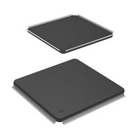
HD6417705F133BV Renesas Electronics America, HD6417705F133BV Datasheet - Page 45

HD6417705F133BV
Manufacturer Part Number
HD6417705F133BV
Description
MPU 3V 0K PB-FREE 208 FP
Manufacturer
Renesas Electronics America
Series
SuperH® SH7700r
Datasheet
1.HD6417705F133BV.pdf
(741 pages)
Specifications of HD6417705F133BV
Core Processor
SH-3
Core Size
32-Bit
Speed
133MHz
Connectivity
EBI/EMI, FIFO, IrDA, SCI, USB
Peripherals
DMA, POR, PWM, WDT
Number Of I /o
105
Program Memory Type
ROMless
Ram Size
32K x 8
Voltage - Supply (vcc/vdd)
1.4 V ~ 1.6 V
Data Converters
A/D 4x10b
Oscillator Type
Internal
Operating Temperature
-20°C ~ 75°C
Package / Case
208-LQFP
Lead Free Status / RoHS Status
Lead free / RoHS Compliant
Eeprom Size
-
Program Memory Size
-
- Current page: 45 of 741
- Download datasheet (5Mb)
Section 7 Bus State Controller (BSC)
Table 7.1
Table 7.2
Table 7.3
Table 7.4
Table 7.5
Table 7.6
Table 7.7
Table 7.8
Table 7.9
Table 7.10
Table 7.11
Table 7.12
Table 7.13
Table 7.14
Table 7.15
Table 7.16
Table 7.17
Table 7.18
Section 8 Direct Memory Access Controller (DMAC)
Table 8.1
Table 8.2
Table 8.3
Table 8.4
Table 8.5
Table 8.6
Table 8.7
Table 8.8
Table 8.9
Section 9 Clock Pulse Generator (CPG)
Table 9.1
Table 9.2
Table 9.3
Section 11 Power-Down Modes
Table 11.1
Correspondence between External Pins (MD3 and MD4) and Memory Size .......... 154
32-Bit External Device/Big Endian Access and Data Alignment............................ 181
16-Bit External Device/Big Endian Access and Data Alignment............................ 182
8-Bit External Device/Big Endian Access and Data Alignment ............................. 183
32-Bit External Device/Little Endian Access and Data Alignment......................... 184
16-Bit External Device/Little Endian Access and Data Alignment......................... 185
8-Bit External Device/Little Endian Access and Data Alignment........................... 186
Selecting On-Chip Peripheral Module Request Modes with RS3 to RS0 Bits......... 256
Selecting On-Chip Peripheral Module Request Modes with RS3 to RS0 Bits......... 256
Supported DMA Transfers.................................................................................... 260
Pin Configuration ................................................................................................. 151
Physical Address Space Map ................................................................................ 152
Pin Configuration ................................................................................................. 241
Transfer Request Sources ..................................................................................... 251
Selecting External Request Modes with RS Bits.................................................... 254
Selecting External Request Detection with DL, DS Bits ........................................ 255
Selecting External Request Detection with DO Bit................................................ 255
Relationship of Request Modes and Bus Modes by DMA Transfer Category......... 266
Clock Pulse Generator Pins and Functions ............................................................ 274
Clock Operating Modes........................................................................................ 275
Possible Combination of Clock Modes and FRQCR Values .................................. 276
Relationship between A2/3BSZ[1:0], A2/3ROW[1:0],
and Address Multiplex Output (1)-1.................................................................. 201
Relationship between A2/3BSZ[1:0], A2/3ROW[1:0],
and Address Multiplex Output (2)-1.................................................................. 203
Relationship between A2/3BSZ[1:0], A2/3ROW[1:0],
and Address Multiplex Output (3)..................................................................... 205
Relationship between A2/3BSZ[1:0], A2/3ROW[1:0],
and Address Multiplex Output (4)-1.................................................................. 206
Relationship between A2/3BSZ[1:0], A2/3ROW[1:0],
and Address Multiplex Output (5)-1.................................................................. 208
Relationship between A2/3BSZ[1:0], A2/3ROW[1:0],
and Address Multiplex Output (6)-1.................................................................. 210
Relationship between Access Size and Number of Bursts .................................. 212
Access Address in SDRAM Mode Register Write ............................................. 229
Relationship between Bus Width, Access Size, and Number of Bursts............... 232
States of Power-Down Modes ........................................................................... 294
Rev. 2.00, 09/03, page xliii of xlvi
Related parts for HD6417705F133BV
Image
Part Number
Description
Manufacturer
Datasheet
Request
R

Part Number:
Description:
KIT STARTER FOR M16C/29
Manufacturer:
Renesas Electronics America
Datasheet:

Part Number:
Description:
KIT STARTER FOR R8C/2D
Manufacturer:
Renesas Electronics America
Datasheet:

Part Number:
Description:
R0K33062P STARTER KIT
Manufacturer:
Renesas Electronics America
Datasheet:

Part Number:
Description:
KIT STARTER FOR R8C/23 E8A
Manufacturer:
Renesas Electronics America
Datasheet:

Part Number:
Description:
KIT STARTER FOR R8C/25
Manufacturer:
Renesas Electronics America
Datasheet:

Part Number:
Description:
KIT STARTER H8S2456 SHARPE DSPLY
Manufacturer:
Renesas Electronics America
Datasheet:

Part Number:
Description:
KIT STARTER FOR R8C38C
Manufacturer:
Renesas Electronics America
Datasheet:

Part Number:
Description:
KIT STARTER FOR R8C35C
Manufacturer:
Renesas Electronics America
Datasheet:

Part Number:
Description:
KIT STARTER FOR R8CL3AC+LCD APPS
Manufacturer:
Renesas Electronics America
Datasheet:

Part Number:
Description:
KIT STARTER FOR RX610
Manufacturer:
Renesas Electronics America
Datasheet:

Part Number:
Description:
KIT STARTER FOR R32C/118
Manufacturer:
Renesas Electronics America
Datasheet:

Part Number:
Description:
KIT DEV RSK-R8C/26-29
Manufacturer:
Renesas Electronics America
Datasheet:

Part Number:
Description:
KIT STARTER FOR SH7124
Manufacturer:
Renesas Electronics America
Datasheet:

Part Number:
Description:
KIT STARTER FOR H8SX/1622
Manufacturer:
Renesas Electronics America
Datasheet:

Part Number:
Description:
KIT DEV FOR SH7203
Manufacturer:
Renesas Electronics America
Datasheet:


