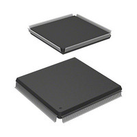
HD6417727F160V Renesas Electronics America, HD6417727F160V Datasheet - Page 361

HD6417727F160V
Manufacturer Part Number
HD6417727F160V
Description
MPU 3V 16K PB-FREE 240-QFP
Manufacturer
Renesas Electronics America
Series
SuperH® SH7700r
Datasheet
1.HD6417727BP100CV.pdf
(1098 pages)
Specifications of HD6417727F160V
Core Processor
SH-3 DSP
Core Size
32-Bit
Speed
160MHz
Connectivity
FIFO, SCI, SIO, SmartCard, USB
Peripherals
DMA, LCD, POR, WDT
Number Of I /o
104
Program Memory Type
ROMless
Ram Size
32K x 8
Voltage - Supply (vcc/vdd)
1.7 V ~ 2.05 V
Data Converters
A/D 6x10b; D/A 2x8b
Oscillator Type
Internal
Operating Temperature
-20°C ~ 75°C
Package / Case
240-QFP
Lead Free Status / RoHS Status
Lead free / RoHS Compliant
Eeprom Size
-
Program Memory Size
-
Available stocks
Company
Part Number
Manufacturer
Quantity
Price
Company:
Part Number:
HD6417727F160V
Manufacturer:
HITACHI
Quantity:
9
Company:
Part Number:
HD6417727F160V
Manufacturer:
Renesas Electronics America
Quantity:
10 000
Part Number:
HD6417727F160V
Manufacturer:
RENESAS/瑞萨
Quantity:
20 000
- Current page: 361 of 1098
- Download datasheet (7Mb)
12.2.5
The individual memory control register (MCR) is a 16-bit read/write register that specifies RAS
and CAS timing and burst control for synchronous DRAM (areas 2 and 3), specifies address
multiplexing, and controls refresh. This enables direct connection of synchronous DRAM without
external circuits.
The MCR is initialized to H'0000 by power-on resets, but is not initialized by manual resets or
standby mode. The bits TPC1 to TPC0, RCD1 to RCD0, TRWL1 to TRWL0, TRAS1 to TRAS0,
AMX3 to AMX0, and are written to at the initialization after a power-on reset and are not then
modified again. When RFSH and RMODE are written to, write the same values to the other bits.
When using synchronous DRAM, do not access areas 2 and 3 until this register is initialized.
Bits 15 and 14—RAS Precharge Time (TPC1, TPC0): These bits set the minimum number of
cycles until output of the next bank-active command after precharge, when the synchronous
DRAM interface is selected for external memory. However, the number of cycles inserted
immediately after the precharge all banks (PALL) command is issued when performing auto-
refresh is one fewer than the number of cycles during normal operation.
Bit 15:
TPC1
0
1
Note: * Immediately after the precharge all banks (PALL) command is issued when performing
Initial value:
R/W: R/W
auto-refresh.
Bit:
Individual Memory Control Register (MCR)
Bit 14:
TPC0
0
1
0
1
TPC1 TPC0 RCD1 RCD0 TRWL
15
0
R/W
14
0
Description
Normal Operation
1 cycle
2 cycles
3 cycles
4 cycles
R/W
13
0
R/W
12
0
(Initial value) 0 cycle
R/W
11
1
0
TRWL
R/W
10
0
0
TRAS
Immediately After
Precharge Command*
1 cycle
2 cycles
3 cycles
R/W
9
1
0
TRAS
R/W
8
0
0
(Initial value)
Rev.6.00 Mar. 27, 2009 Page 303 of 1036
R/W
—
7
0
Section 12 Bus State Controller (BSC)
AMX3 AMX2 AMX1 AMX0 RFSH RMO
R/W
6
0
R/W
5
0
R/W
4
0
Immediately After
Self-refresh
2 cycles
5 cycles
8 cycles
11 cycles
R/W
3
0
REJ09B0254-0600
R/W
2
0
(Initial value)
R/W
DE
1
0
R/W
—
0
0
Related parts for HD6417727F160V
Image
Part Number
Description
Manufacturer
Datasheet
Request
R

Part Number:
Description:
KIT STARTER FOR M16C/29
Manufacturer:
Renesas Electronics America
Datasheet:

Part Number:
Description:
KIT STARTER FOR R8C/2D
Manufacturer:
Renesas Electronics America
Datasheet:

Part Number:
Description:
R0K33062P STARTER KIT
Manufacturer:
Renesas Electronics America
Datasheet:

Part Number:
Description:
KIT STARTER FOR R8C/23 E8A
Manufacturer:
Renesas Electronics America
Datasheet:

Part Number:
Description:
KIT STARTER FOR R8C/25
Manufacturer:
Renesas Electronics America
Datasheet:

Part Number:
Description:
KIT STARTER H8S2456 SHARPE DSPLY
Manufacturer:
Renesas Electronics America
Datasheet:

Part Number:
Description:
KIT STARTER FOR R8C38C
Manufacturer:
Renesas Electronics America
Datasheet:

Part Number:
Description:
KIT STARTER FOR R8C35C
Manufacturer:
Renesas Electronics America
Datasheet:

Part Number:
Description:
KIT STARTER FOR R8CL3AC+LCD APPS
Manufacturer:
Renesas Electronics America
Datasheet:

Part Number:
Description:
KIT STARTER FOR RX610
Manufacturer:
Renesas Electronics America
Datasheet:

Part Number:
Description:
KIT STARTER FOR R32C/118
Manufacturer:
Renesas Electronics America
Datasheet:

Part Number:
Description:
KIT DEV RSK-R8C/26-29
Manufacturer:
Renesas Electronics America
Datasheet:

Part Number:
Description:
KIT STARTER FOR SH7124
Manufacturer:
Renesas Electronics America
Datasheet:

Part Number:
Description:
KIT STARTER FOR H8SX/1622
Manufacturer:
Renesas Electronics America
Datasheet:

Part Number:
Description:
KIT DEV FOR SH7203
Manufacturer:
Renesas Electronics America
Datasheet:


