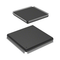
HD6417727F160V Renesas Electronics America, HD6417727F160V Datasheet - Page 571

HD6417727F160V
Manufacturer Part Number
HD6417727F160V
Description
MPU 3V 16K PB-FREE 240-QFP
Manufacturer
Renesas Electronics America
Series
SuperH® SH7700r
Datasheet
1.HD6417727BP100CV.pdf
(1098 pages)
Specifications of HD6417727F160V
Core Processor
SH-3 DSP
Core Size
32-Bit
Speed
160MHz
Connectivity
FIFO, SCI, SIO, SmartCard, USB
Peripherals
DMA, LCD, POR, WDT
Number Of I /o
104
Program Memory Type
ROMless
Ram Size
32K x 8
Voltage - Supply (vcc/vdd)
1.7 V ~ 2.05 V
Data Converters
A/D 6x10b; D/A 2x8b
Oscillator Type
Internal
Operating Temperature
-20°C ~ 75°C
Package / Case
240-QFP
Lead Free Status / RoHS Status
Lead free / RoHS Compliant
Eeprom Size
-
Program Memory Size
-
Available stocks
Company
Part Number
Manufacturer
Quantity
Price
Company:
Part Number:
HD6417727F160V
Manufacturer:
HITACHI
Quantity:
9
Company:
Part Number:
HD6417727F160V
Manufacturer:
Renesas Electronics America
Quantity:
10 000
Part Number:
HD6417727F160V
Manufacturer:
RENESAS/瑞萨
Quantity:
20 000
- Current page: 571 of 1098
- Download datasheet (7Mb)
Section 17 Serial Communication Interface (SCI)
Clock
An internal clock generated by the on-chip baud rate generator or an external clock input from the
SCK0 pin can be selected as the SCI transmit/receive clock. The clock source is selected by the
C/A bit in the serial mode register (SCSMR) and bits CKE1 and CKE0 in the serial control
register (SCSCR) (table 17.10).
When an external clock is input at the SCK0 pin, it must have a frequency equal to 16 times the
desired bit rate.
When the SCI operates on an internal clock, it can output a clock signal at the SCK0 pin. The
frequency of this output clock is equal to the bit rate. The phase is aligned as in figure 17.6 so that
the rising edge of the clock occurs at the center of each transmit data bit.
0
D0
D1
D2
D3
D4
D5
D6
D7
0/1
1
1
1 frame
Figure 17.6 Relationship between Output Clock and Transfer Data Phase
(Asynchronous Mode)
Transmitting and Receiving Data
SCI Initialization (Asynchronous Mode):
Before transmitting or receiving, clear the TE and RE bits to 0 in the serial control register
(SCSCR), then initialize the SCI as follows.
When changing the operation mode or communication format, always clear the TE and RE bits to
0 before following the procedure given below. Clearing TE to 0 sets TDRE to 1 and initializes the
transmit shift register (SCTSR). Clearing RE to 0, however, does not initialize the RDRF, PER,
FER, and ORER flags or receive data register (SCRDR), which retain their previous contents.
When an external clock is used, the clock should not be stopped during initialization or subsequent
operation. SCI operation becomes unreliable if the clock is stopped.
Figure 17.7 is a sample flowchart for initializing the SCI. The procedure for initializing the SCI is:
Rev.6.00 Mar. 27, 2009 Page 513 of 1036
REJ09B0254-0600
Related parts for HD6417727F160V
Image
Part Number
Description
Manufacturer
Datasheet
Request
R

Part Number:
Description:
KIT STARTER FOR M16C/29
Manufacturer:
Renesas Electronics America
Datasheet:

Part Number:
Description:
KIT STARTER FOR R8C/2D
Manufacturer:
Renesas Electronics America
Datasheet:

Part Number:
Description:
R0K33062P STARTER KIT
Manufacturer:
Renesas Electronics America
Datasheet:

Part Number:
Description:
KIT STARTER FOR R8C/23 E8A
Manufacturer:
Renesas Electronics America
Datasheet:

Part Number:
Description:
KIT STARTER FOR R8C/25
Manufacturer:
Renesas Electronics America
Datasheet:

Part Number:
Description:
KIT STARTER H8S2456 SHARPE DSPLY
Manufacturer:
Renesas Electronics America
Datasheet:

Part Number:
Description:
KIT STARTER FOR R8C38C
Manufacturer:
Renesas Electronics America
Datasheet:

Part Number:
Description:
KIT STARTER FOR R8C35C
Manufacturer:
Renesas Electronics America
Datasheet:

Part Number:
Description:
KIT STARTER FOR R8CL3AC+LCD APPS
Manufacturer:
Renesas Electronics America
Datasheet:

Part Number:
Description:
KIT STARTER FOR RX610
Manufacturer:
Renesas Electronics America
Datasheet:

Part Number:
Description:
KIT STARTER FOR R32C/118
Manufacturer:
Renesas Electronics America
Datasheet:

Part Number:
Description:
KIT DEV RSK-R8C/26-29
Manufacturer:
Renesas Electronics America
Datasheet:

Part Number:
Description:
KIT STARTER FOR SH7124
Manufacturer:
Renesas Electronics America
Datasheet:

Part Number:
Description:
KIT STARTER FOR H8SX/1622
Manufacturer:
Renesas Electronics America
Datasheet:

Part Number:
Description:
KIT DEV FOR SH7203
Manufacturer:
Renesas Electronics America
Datasheet:


