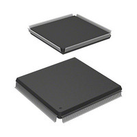
HD6417727F160V Renesas Electronics America, HD6417727F160V Datasheet - Page 49

HD6417727F160V
Manufacturer Part Number
HD6417727F160V
Description
MPU 3V 16K PB-FREE 240-QFP
Manufacturer
Renesas Electronics America
Series
SuperH® SH7700r
Datasheet
1.HD6417727BP100CV.pdf
(1098 pages)
Specifications of HD6417727F160V
Core Processor
SH-3 DSP
Core Size
32-Bit
Speed
160MHz
Connectivity
FIFO, SCI, SIO, SmartCard, USB
Peripherals
DMA, LCD, POR, WDT
Number Of I /o
104
Program Memory Type
ROMless
Ram Size
32K x 8
Voltage - Supply (vcc/vdd)
1.7 V ~ 2.05 V
Data Converters
A/D 6x10b; D/A 2x8b
Oscillator Type
Internal
Operating Temperature
-20°C ~ 75°C
Package / Case
240-QFP
Lead Free Status / RoHS Status
Lead free / RoHS Compliant
Eeprom Size
-
Program Memory Size
-
Available stocks
Company
Part Number
Manufacturer
Quantity
Price
Company:
Part Number:
HD6417727F160V
Manufacturer:
HITACHI
Quantity:
9
Company:
Part Number:
HD6417727F160V
Manufacturer:
Renesas Electronics America
Quantity:
10 000
Part Number:
HD6417727F160V
Manufacturer:
RENESAS/瑞萨
Quantity:
20 000
- Current page: 49 of 1098
- Download datasheet (7Mb)
Figure 32.26 Synchronous DRAM Read Bus Cycle (Burst Read (Single Read × 4),
Figure 32.27 Synchronous DRAM Write Bus Cycle (RCD = 0, TPC = 0, TRWL = 0).............. 961
Figure 32.28 Synchronous DRAM Write Bus Cycle (RCD = 2, TPC = 1, TRWL = 1).............. 962
Figure 32.29 Synchronous DRAM Write Bus Cycle (Burst Mode (Single Write × 4),
Figure 32.30 Synchronous DRAM Write Bus Cycle (Burst Mode (Single Write × 4),
Figure 32.31 Synchronous DRAM Auto-Refresh Cycle (TRAS = 1, TPC = 1).......................... 965
Figure 32.32 Synchronous DRAM Self-Refresh Cycle (TPC = 0).............................................. 966
Figure 32.33 Synchronous DRAM Mode Register Write Cycle ................................................. 967
Figure 32.34 PCMCIA Memory Bus Cycle (TED = 0, TEH = 0, No Wait) ............................... 968
Figure 32.35 PCMCIA Memory Bus Cycle
Figure 32.36 PCMCIA Memory Bus Cycle (Burst Read, TED = 0, TEH = 0, No Wait)............ 970
Figure 32.37 PCMCIA Memory Bus Cycle
Figure 32.38 PCMCIA I/O Bus Cycle (TED = 0, TEH = 0, No Wait)........................................ 972
Figure 32.39 PCMCIA I/O Bus Cycle
Figure 32.40 PCMCIA I/O Bus Cycle
Figure 32.41 Oscillation Settling Time at RTC Crystal Oscillator Power-on ............................. 976
Figure 32.42 SCK Input Clock Timing ....................................................................................... 976
Figure 32.43 SCI I/O Timing in Clock Synchronous Mode ........................................................ 976
Figure 32.44 I/O Port Timing ...................................................................................................... 977
Figure 32.45 DREQ Input Timing............................................................................................... 977
Figure 32.46 DRAK Output Timing............................................................................................ 977
Figure 32.47 TCK Input Timing.................................................................................................. 978
Figure 32.48 TRST Input Timing (Reset Hold)........................................................................... 979
Figure 32.49 H-UDI Data Transfer Timing................................................................................. 979
Figure 32.50 ASEMD0 Input Timing.......................................................................................... 979
Figure 32.51 LCDC AC Specification......................................................................................... 981
Figure 32.52 SIOMCLK Input Timing........................................................................................ 982
Figure 32.53 SIOF Transmit/Receive Timing (Master Mode 1: Fall Sampling Time) ............... 983
Figure 32.54 SIOF Transmit/Receive Timing (Master Mode 1: Rise Sampling Time)............... 983
Figure 32.55 SIOF Transmit/Receive Timing (Master Mode 2: Fall Sampling Time) ............... 984
Figure 32.56 SIOF Transmit/Receive Timing (Master Mode 2: Rise Sampling Time)............... 984
Figure 32.57 SIOF Transmit/Receive Timing (Slave Mode 1 and Slave Mode 2)...................... 985
Figure 32.58 USB Clock Timing................................................................................................. 985
Figure 32.59 AFEIF Module AC Timing .................................................................................... 988
RCD = 1, CAS Latency = 3, TPC = 0) ................................................................... 960
RCD = 0, TPC = 1, TRWL = 0) ............................................................................. 963
RCD = 1, TPC = 0, TRWL = 0) ............................................................................. 964
(TED = 2, TEH = 1, One Wait, External Wait, WAITSEL = 1) ............................ 969
(Burst Read, TED = 1, TEH = 1, Two Waits, Burst Pitch = 3, WAITSEL = 1) .... 971
(TED = 2, TEH = 1, One Wait, External Wait, WAITSEL = 1) ............................ 973
(TED = 1, TEH = 1, One Wait, Bus Sizing, WAITSEL = 1) ................................. 974
Rev.6.00 Mar. 27, 2009 Page xlvii of lvi
REJ09B0254-0600
Related parts for HD6417727F160V
Image
Part Number
Description
Manufacturer
Datasheet
Request
R

Part Number:
Description:
KIT STARTER FOR M16C/29
Manufacturer:
Renesas Electronics America
Datasheet:

Part Number:
Description:
KIT STARTER FOR R8C/2D
Manufacturer:
Renesas Electronics America
Datasheet:

Part Number:
Description:
R0K33062P STARTER KIT
Manufacturer:
Renesas Electronics America
Datasheet:

Part Number:
Description:
KIT STARTER FOR R8C/23 E8A
Manufacturer:
Renesas Electronics America
Datasheet:

Part Number:
Description:
KIT STARTER FOR R8C/25
Manufacturer:
Renesas Electronics America
Datasheet:

Part Number:
Description:
KIT STARTER H8S2456 SHARPE DSPLY
Manufacturer:
Renesas Electronics America
Datasheet:

Part Number:
Description:
KIT STARTER FOR R8C38C
Manufacturer:
Renesas Electronics America
Datasheet:

Part Number:
Description:
KIT STARTER FOR R8C35C
Manufacturer:
Renesas Electronics America
Datasheet:

Part Number:
Description:
KIT STARTER FOR R8CL3AC+LCD APPS
Manufacturer:
Renesas Electronics America
Datasheet:

Part Number:
Description:
KIT STARTER FOR RX610
Manufacturer:
Renesas Electronics America
Datasheet:

Part Number:
Description:
KIT STARTER FOR R32C/118
Manufacturer:
Renesas Electronics America
Datasheet:

Part Number:
Description:
KIT DEV RSK-R8C/26-29
Manufacturer:
Renesas Electronics America
Datasheet:

Part Number:
Description:
KIT STARTER FOR SH7124
Manufacturer:
Renesas Electronics America
Datasheet:

Part Number:
Description:
KIT STARTER FOR H8SX/1622
Manufacturer:
Renesas Electronics America
Datasheet:

Part Number:
Description:
KIT DEV FOR SH7203
Manufacturer:
Renesas Electronics America
Datasheet:


