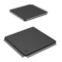
HD6417706F133 Renesas Electronics America, HD6417706F133 Datasheet - Page 269

HD6417706F133
Manufacturer Part Number
HD6417706F133
Description
IC SUPERH MPU ROMLESS 176LQFP
Manufacturer
Renesas Electronics America
Series
SuperH® SH7700r
Datasheet
1.HD6417706F133V.pdf
(751 pages)
Specifications of HD6417706F133
Core Processor
SH-3
Core Size
32-Bit
Speed
133MHz
Connectivity
EBI/EMI, FIFO, SCI, SmartCard
Peripherals
DMA, POR, WDT
Number Of I /o
103
Program Memory Type
ROMless
Ram Size
16K x 8
Voltage - Supply (vcc/vdd)
1.75 V ~ 2.05 V
Oscillator Type
Internal
Operating Temperature
-20°C ~ 75°C
Package / Case
176-LQFP
Lead Free Status / RoHS Status
Contains lead / RoHS non-compliant
Eeprom Size
-
Program Memory Size
-
Data Converters
-
Available stocks
Company
Part Number
Manufacturer
Quantity
Price
Part Number:
HD6417706F133
Manufacturer:
RENESAS/瑞萨
Quantity:
20 000
Company:
Part Number:
HD6417706F133V
Manufacturer:
EDISON
Quantity:
2 000
Company:
Part Number:
HD6417706F133V
Manufacturer:
Renesas Electronics America
Quantity:
10 000
Part Number:
HD6417706F133V
Manufacturer:
RENESAS/瑞萨
Quantity:
20 000
- Current page: 269 of 751
- Download datasheet (5Mb)
Tc1, Tc2, and Tc3 cycles, and a WRITA command that performs auto-precharge is issued in the
Tc4 cycle. In the write cycle, the write data is output at the same time as the write command. In
case of the write with auto-precharge command, precharging of the relevant bank is performed in
the synchronous DRAM after completion of the write command, and therefore no command can
be issued for the same bank until precharging is completed. Consequently, in addition to the
precharge wait cycle, Tpc, used in a read access, cycle Trwl is also added as a wait interval until
precharging is started following the write command. Issuance of a new command for the same
bank is postponed during this interval. The number of Trwl cycles can be specified by the TRWL
bit in MCR.
CKIO
Address
upper bits
A12 or A11 *
Address
lower bits *
CSn
RD/WR
RASx
CASx
DQMxx
D31 to D0
(read)
BS
Notes: 1.
Figure 8.16 Basic Timing for Synchronous DRAM Burst Write
2.
2
Command bit
Column address
1
Tr
Tc1
Tc2
Tc3
Rev. 5.00 May 29, 2006 page 219 of 698
Section 8 Bus State Controller (BSC)
Tc4
(Trw1)
REJ09B0146-0500
(Tpc)
Related parts for HD6417706F133
Image
Part Number
Description
Manufacturer
Datasheet
Request
R

Part Number:
Description:
KIT STARTER FOR M16C/29
Manufacturer:
Renesas Electronics America
Datasheet:

Part Number:
Description:
KIT STARTER FOR R8C/2D
Manufacturer:
Renesas Electronics America
Datasheet:

Part Number:
Description:
R0K33062P STARTER KIT
Manufacturer:
Renesas Electronics America
Datasheet:

Part Number:
Description:
KIT STARTER FOR R8C/23 E8A
Manufacturer:
Renesas Electronics America
Datasheet:

Part Number:
Description:
KIT STARTER FOR R8C/25
Manufacturer:
Renesas Electronics America
Datasheet:

Part Number:
Description:
KIT STARTER H8S2456 SHARPE DSPLY
Manufacturer:
Renesas Electronics America
Datasheet:

Part Number:
Description:
KIT STARTER FOR R8C38C
Manufacturer:
Renesas Electronics America
Datasheet:

Part Number:
Description:
KIT STARTER FOR R8C35C
Manufacturer:
Renesas Electronics America
Datasheet:

Part Number:
Description:
KIT STARTER FOR R8CL3AC+LCD APPS
Manufacturer:
Renesas Electronics America
Datasheet:

Part Number:
Description:
KIT STARTER FOR RX610
Manufacturer:
Renesas Electronics America
Datasheet:

Part Number:
Description:
KIT STARTER FOR R32C/118
Manufacturer:
Renesas Electronics America
Datasheet:

Part Number:
Description:
KIT DEV RSK-R8C/26-29
Manufacturer:
Renesas Electronics America
Datasheet:

Part Number:
Description:
KIT STARTER FOR SH7124
Manufacturer:
Renesas Electronics America
Datasheet:

Part Number:
Description:
KIT STARTER FOR H8SX/1622
Manufacturer:
Renesas Electronics America
Datasheet:

Part Number:
Description:
KIT DEV FOR SH7203
Manufacturer:
Renesas Electronics America
Datasheet:


