MC9S12XDP512MAG Freescale, MC9S12XDP512MAG Datasheet - Page 1014
MC9S12XDP512MAG
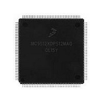
Manufacturer Part Number
MC9S12XDP512MAG
Description
Manufacturer
Freescale
Datasheet
1.MC9S12XDP512MAG.pdf
(1348 pages)
Specifications of MC9S12XDP512MAG
Cpu Family
HCS12
Device Core Size
16b
Frequency (max)
40MHz
Interface Type
CAN/I2C/SCI/SPI
Total Internal Ram Size
32KB
# I/os (max)
119
Number Of Timers - General Purpose
12
Operating Supply Voltage (typ)
2.5/5V
Operating Supply Voltage (max)
2.75/5.5V
Operating Supply Voltage (min)
2.35/3.15V
On-chip Adc
2(24-chx10-bit)
Instruction Set Architecture
CISC
Operating Temp Range
-40C to 125C
Operating Temperature Classification
Automotive
Mounting
Surface Mount
Pin Count
144
Package Type
LQFP
Program Memory Type
Flash
Program Memory Size
512KB
Lead Free Status / RoHS Status
Compliant
Available stocks
Company
Part Number
Manufacturer
Quantity
Price
Company:

Part Number:
MC9S12XDP512MAG
Manufacturer:
FREESCALE
Quantity:
5 530
Company:
Part Number:
MC9S12XDP512MAG
Manufacturer:
Exar
Quantity:
20
Company:
Part Number:
MC9S12XDP512MAG
Manufacturer:
Freescale Semiconductor
Quantity:
10 000


Chapter 24 DG128 Port Integration Module (S12XDG128PIMV2)
24.0.5.42 Port H Data Register (PTH)
Read: Anytime.
Write: Anytime.
Port H pins 7–0 are associated with the routed SPI1.
These pins can be used as general purpose I/O when not used with any of the peripherals.
If the data direction bits of the associated I/O pins are set to logic level “1”, a read returns the value of the
port register, otherwise the buffered pin input state is read.
The routed SPI1 function takes precedence over the general purpose I/O function if the routed SPI1 is
enabled. Refer to SPI section for details.
24.0.5.43 Port H Input Register (PTIH)
Read: Anytime.
Write: Never, writes to this register have no effect.
1016
Routed
PIFP[7:0]
Reset
Reset
Field
1. These registers are reset to zero. Two bus clock cycles after reset release the register values are updated with the
7–0
SPI
W
W
associated pin values.
R
R
1
PTIH7
PTH7
Interrupt Flags Port P
0 No active edge pending. Writing a “0” has no effect.
1 Active edge on the associated bit has occurred (an interrupt will occur if the associated enable bit is set).
—
0
7
7
Writing a logic level “1” clears the associated flag.
= Unimplemented or Reserved
PTIH6
PTH6
—
0
6
6
Figure 24-45. Port H Input Register (PTIH)
Figure 24-44. Port H Data Register (PTH)
Table 24-40. PIFP Field Descriptions
MC9S12XDP512 Data Sheet, Rev. 2.21
PTIH5
PTH5
—
0
5
5
PTIH4
PTH4
—
0
4
4
Description
PTIH3
PTH3
SS1
—
0
3
3
PTIH2
SCK1
PTH2
—
0
2
2
Freescale Semiconductor
MOSI1
PTIH1
PTH1
—
0
1
1
MISO1
PTIH0
PTH0
—
0
0
0
Related parts for MC9S12XDP512MAG
Image
Part Number
Description
Manufacturer
Datasheet
Request
R

Part Number:
Description:
16-BIT MICROPROCESSOR FAMILY
Manufacturer:
FREESCALE [Freescale Semiconductor, Inc]
Datasheet:

Part Number:
Description:
TOWER ELEVATOR BOARDS HARDWARE
Manufacturer:
Freescale Semiconductor
Datasheet:

Part Number:
Description:
TOWER SERIAL I/O HARDWARE
Manufacturer:
Freescale Semiconductor
Datasheet:

Part Number:
Description:
LCD MODULE FOR TWR SYSTEM
Manufacturer:
Freescale Semiconductor
Datasheet:

Part Number:
Description:
DAUGHTER LCD WVGA I.MX51
Manufacturer:
Freescale Semiconductor
Datasheet:

Part Number:
Description:
TOWER SYSTEM BOARD MPC5125
Manufacturer:
Freescale Semiconductor
Datasheet:

Part Number:
Description:
KIT EVALUATION I.MX51
Manufacturer:
Freescale Semiconductor
Datasheet:

Part Number:
Description:
KIT DEVELOPMENT WINCE IMX25
Manufacturer:
Freescale Semiconductor
Datasheet:

Part Number:
Description:
TOWER SYSTEM KIT MPC5125
Manufacturer:
Freescale Semiconductor
Datasheet:

Part Number:
Description:
TOWER SYSTEM BOARD K40X256
Manufacturer:
Freescale Semiconductor
Datasheet:

Part Number:
Description:
TOWER SYSTEM KIT K40X256
Manufacturer:
Freescale Semiconductor
Datasheet:

Part Number:
Description:
Microcontrollers (MCU) MX28 PLATFORM DEV KIT
Manufacturer:
Freescale Semiconductor
Datasheet:

Part Number:
Description:
MCU, MPU & DSP Development Tools IAR KickStart Kit for Kinetis K60
Manufacturer:
Freescale Semiconductor
Datasheet:

Part Number:
Description:
24BIT HDMI MX535/08
Manufacturer:
Freescale Semiconductor
Datasheet:

Part Number:
Description:
Manufacturer:
Freescale Semiconductor, Inc
Datasheet: