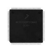
MC9S12XDP512MAG Freescale, MC9S12XDP512MAG Datasheet - Page 503

MC9S12XDP512MAG
Manufacturer Part Number
MC9S12XDP512MAG
Description
Manufacturer
Freescale
Datasheet
1.MC9S12XDP512MAG.pdf
(1348 pages)
Specifications of MC9S12XDP512MAG
Cpu Family
HCS12
Device Core Size
16b
Frequency (max)
40MHz
Interface Type
CAN/I2C/SCI/SPI
Total Internal Ram Size
32KB
# I/os (max)
119
Number Of Timers - General Purpose
12
Operating Supply Voltage (typ)
2.5/5V
Operating Supply Voltage (max)
2.75/5.5V
Operating Supply Voltage (min)
2.35/3.15V
On-chip Adc
2(24-chx10-bit)
Instruction Set Architecture
CISC
Operating Temp Range
-40C to 125C
Operating Temperature Classification
Automotive
Mounting
Surface Mount
Pin Count
144
Package Type
LQFP
Program Memory Type
Flash
Program Memory Size
512KB
Lead Free Status / RoHS Status
Compliant
Available stocks
Company
Part Number
Manufacturer
Quantity
Price
Company:
Part Number:
MC9S12XDP512MAG
Manufacturer:
FREESCALE
Quantity:
5 530
Company:
Part Number:
MC9S12XDP512MAG
Manufacturer:
Exar
Quantity:
20
Company:
Part Number:
MC9S12XDP512MAG
Manufacturer:
Freescale Semiconductor
Quantity:
10 000
- Current page: 503 of 1348
- Download datasheet (8Mb)
indicating that the received byte can be read. If the receive interrupt enable bit, RIE, in SCI control
register 2 (SCICR2) is also set, the RDRF flag generates an RDRF interrupt request.
11.4.6.3
The RT clock rate. The RT clock is an internal signal with a frequency 16 times the baud rate. To adjust
for baud rate mismatch, the RT clock (see
To locate the start bit, data recovery logic does an asynchronous search for a logic 0 preceded by three logic
1s.When the falling edge of a possible start bit occurs, the RT clock begins to count to 16.
To verify the start bit and to detect noise, data recovery logic takes samples at RT3, RT5, and RT7.
Figure 11-16
If start bit verification is not successful, the RT clock is reset and a new search for a start bit begins.
Freescale Semiconductor
RT CLock Count
•
•
Reset RT Clock
After every start bit
After the receiver detects a data bit change from logic 1 to logic 0 (after the majority of data bit
samples at RT8, RT9, and RT10 returns a valid logic 1 and the majority of the next RT8, RT9, and
RT10 samples returns a valid logic 0)
RT Clock
Samples
RXD
Data Sampling
summarizes the results of the start bit verification samples.
1
RT3, RT5, and RT7 Samples
1
1
1
000
001
010
011
100
101
110
111
1
1
Figure 11-21. Receiver Data Sampling
Qualification
MC9S12XDP512 Data Sheet, Rev. 2.21
Start Bit
Table 11-16. Start Bit Verification
1
1
Figure
0
0
11-21) is re-synchronized:
Start Bit Verification
Verification
Start Bit
0
Yes
Yes
Yes
Yes
No
No
No
No
0
Chapter 11 Serial Communication Interface (S12SCIV5)
Start Bit
0
Sampling
Data
0
0
Noise Flag
0
1
1
0
1
0
0
0
LSB
503
Related parts for MC9S12XDP512MAG
Image
Part Number
Description
Manufacturer
Datasheet
Request
R

Part Number:
Description:
16-BIT MICROPROCESSOR FAMILY
Manufacturer:
FREESCALE [Freescale Semiconductor, Inc]
Datasheet:

Part Number:
Description:
TOWER ELEVATOR BOARDS HARDWARE
Manufacturer:
Freescale Semiconductor
Datasheet:

Part Number:
Description:
TOWER SERIAL I/O HARDWARE
Manufacturer:
Freescale Semiconductor
Datasheet:

Part Number:
Description:
LCD MODULE FOR TWR SYSTEM
Manufacturer:
Freescale Semiconductor
Datasheet:

Part Number:
Description:
DAUGHTER LCD WVGA I.MX51
Manufacturer:
Freescale Semiconductor
Datasheet:

Part Number:
Description:
TOWER SYSTEM BOARD MPC5125
Manufacturer:
Freescale Semiconductor
Datasheet:

Part Number:
Description:
KIT EVALUATION I.MX51
Manufacturer:
Freescale Semiconductor
Datasheet:

Part Number:
Description:
KIT DEVELOPMENT WINCE IMX25
Manufacturer:
Freescale Semiconductor
Datasheet:

Part Number:
Description:
TOWER SYSTEM KIT MPC5125
Manufacturer:
Freescale Semiconductor
Datasheet:

Part Number:
Description:
TOWER SYSTEM BOARD K40X256
Manufacturer:
Freescale Semiconductor
Datasheet:

Part Number:
Description:
TOWER SYSTEM KIT K40X256
Manufacturer:
Freescale Semiconductor
Datasheet:

Part Number:
Description:
Microcontrollers (MCU) MX28 PLATFORM DEV KIT
Manufacturer:
Freescale Semiconductor
Datasheet:

Part Number:
Description:
MCU, MPU & DSP Development Tools IAR KickStart Kit for Kinetis K60
Manufacturer:
Freescale Semiconductor
Datasheet:

Part Number:
Description:
24BIT HDMI MX535/08
Manufacturer:
Freescale Semiconductor
Datasheet:
Part Number:
Description:
Manufacturer:
Freescale Semiconductor, Inc
Datasheet:


