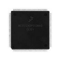
MC9S12XDP512MAG Freescale, MC9S12XDP512MAG Datasheet - Page 1237

MC9S12XDP512MAG
Manufacturer Part Number
MC9S12XDP512MAG
Description
Manufacturer
Freescale
Datasheet
1.MC9S12XDP512MAG.pdf
(1348 pages)
Specifications of MC9S12XDP512MAG
Cpu Family
HCS12
Device Core Size
16b
Frequency (max)
40MHz
Interface Type
CAN/I2C/SCI/SPI
Total Internal Ram Size
32KB
# I/os (max)
119
Number Of Timers - General Purpose
12
Operating Supply Voltage (typ)
2.5/5V
Operating Supply Voltage (max)
2.75/5.5V
Operating Supply Voltage (min)
2.35/3.15V
On-chip Adc
2(24-chx10-bit)
Instruction Set Architecture
CISC
Operating Temp Range
-40C to 125C
Operating Temperature Classification
Automotive
Mounting
Surface Mount
Pin Count
144
Package Type
LQFP
Program Memory Type
Flash
Program Memory Size
512KB
Lead Free Status / RoHS Status
Compliant
Available stocks
Company
Part Number
Manufacturer
Quantity
Price
Company:
Part Number:
MC9S12XDP512MAG
Manufacturer:
FREESCALE
Quantity:
5 530
Company:
Part Number:
MC9S12XDP512MAG
Manufacturer:
Exar
Quantity:
20
Company:
Part Number:
MC9S12XDP512MAG
Manufacturer:
Freescale Semiconductor
Quantity:
10 000
- Current page: 1237 of 1348
- Download datasheet (8Mb)
Appendix A
Electrical Characteristics
A.1
This supplement contains the most accurate electrical information for the S12XD, S12XB & S12XA
families microcontroller available at the time of publication.
This introduction is intended to give an overview on several common topics like power supply, current
injection etc.
A.1.1
The electrical parameters shown in this supplement are guaranteed by various methods. To give the
customer a better understanding the following classification is used and the parameters are tagged
accordingly in the tables where appropriate.
P:
C:
T:
D:
A.1.2
The MC9S12XDP512RMV2 utilizes several pins to supply power to the I/O ports, A/D converter,
oscillator, and PLL as well as the digital core.
The V
The V
regulator.
V
oscillator and the PLL.
V
V
protection.
Freescale Semiconductor
DD1
SS1
DDA
, V
and V
, V
DDA
DDX
Those parameters are guaranteed during production testing on each individual device.
Those parameters are achieved by the design characterization by measuring a statistically relevant
sample size across process variations.
Those parameters are achieved by design characterization on a small sample size from typical
devices under typical conditions unless otherwise noted. All values shown in the typical column
are within this category.
Those parameters are derived mainly from simulations.
SS1
DDX
General
, V
, V
SS2
, V
Parameter Classification
Power Supply
, V
SSA
SSX
This classification is shown in the column labeled “C” in the parameter
tables where appropriate.
DD2
are internally connected by metal.
DDR
, V
pair supplies the A/D converter and parts of the internal voltage regulator.
, and V
DDR
as well as V
, and V
SS2
are the supply pins for the digital logic, V
SSR
SSA
MC9S12XDP512 Data Sheet, Rev. 2.21
pairs supply the I/O pins, V
, V
SSX
, V
SSR
NOTE
are connected by anti-parallel diodes for ESD
DDR
supplies also the internal voltage
DDPLL
Appendix A Electrical Characteristics
, V
SSPLL
supply the
1239
Related parts for MC9S12XDP512MAG
Image
Part Number
Description
Manufacturer
Datasheet
Request
R

Part Number:
Description:
16-BIT MICROPROCESSOR FAMILY
Manufacturer:
FREESCALE [Freescale Semiconductor, Inc]
Datasheet:

Part Number:
Description:
TOWER ELEVATOR BOARDS HARDWARE
Manufacturer:
Freescale Semiconductor
Datasheet:

Part Number:
Description:
TOWER SERIAL I/O HARDWARE
Manufacturer:
Freescale Semiconductor
Datasheet:

Part Number:
Description:
LCD MODULE FOR TWR SYSTEM
Manufacturer:
Freescale Semiconductor
Datasheet:

Part Number:
Description:
DAUGHTER LCD WVGA I.MX51
Manufacturer:
Freescale Semiconductor
Datasheet:

Part Number:
Description:
TOWER SYSTEM BOARD MPC5125
Manufacturer:
Freescale Semiconductor
Datasheet:

Part Number:
Description:
KIT EVALUATION I.MX51
Manufacturer:
Freescale Semiconductor
Datasheet:

Part Number:
Description:
KIT DEVELOPMENT WINCE IMX25
Manufacturer:
Freescale Semiconductor
Datasheet:

Part Number:
Description:
TOWER SYSTEM KIT MPC5125
Manufacturer:
Freescale Semiconductor
Datasheet:

Part Number:
Description:
TOWER SYSTEM BOARD K40X256
Manufacturer:
Freescale Semiconductor
Datasheet:

Part Number:
Description:
TOWER SYSTEM KIT K40X256
Manufacturer:
Freescale Semiconductor
Datasheet:

Part Number:
Description:
Microcontrollers (MCU) MX28 PLATFORM DEV KIT
Manufacturer:
Freescale Semiconductor
Datasheet:

Part Number:
Description:
MCU, MPU & DSP Development Tools IAR KickStart Kit for Kinetis K60
Manufacturer:
Freescale Semiconductor
Datasheet:

Part Number:
Description:
24BIT HDMI MX535/08
Manufacturer:
Freescale Semiconductor
Datasheet:
Part Number:
Description:
Manufacturer:
Freescale Semiconductor, Inc
Datasheet:


