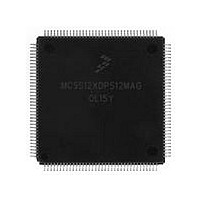
MC9S12XDP512MAG Freescale, MC9S12XDP512MAG Datasheet - Page 85

MC9S12XDP512MAG
Manufacturer Part Number
MC9S12XDP512MAG
Description
Manufacturer
Freescale
Datasheet
1.MC9S12XDP512MAG.pdf
(1348 pages)
Specifications of MC9S12XDP512MAG
Cpu Family
HCS12
Device Core Size
16b
Frequency (max)
40MHz
Interface Type
CAN/I2C/SCI/SPI
Total Internal Ram Size
32KB
# I/os (max)
119
Number Of Timers - General Purpose
12
Operating Supply Voltage (typ)
2.5/5V
Operating Supply Voltage (max)
2.75/5.5V
Operating Supply Voltage (min)
2.35/3.15V
On-chip Adc
2(24-chx10-bit)
Instruction Set Architecture
CISC
Operating Temp Range
-40C to 125C
Operating Temperature Classification
Automotive
Mounting
Surface Mount
Pin Count
144
Package Type
LQFP
Program Memory Type
Flash
Program Memory Size
512KB
Lead Free Status / RoHS Status
Compliant
Available stocks
Company
Part Number
Manufacturer
Quantity
Price
Company:
Part Number:
MC9S12XDP512MAG
Manufacturer:
FREESCALE
Quantity:
5 530
Company:
Part Number:
MC9S12XDP512MAG
Manufacturer:
Exar
Quantity:
20
Company:
Part Number:
MC9S12XDP512MAG
Manufacturer:
Freescale Semiconductor
Quantity:
10 000
- Current page: 85 of 1348
- Download datasheet (8Mb)
2.3.2.1
The SYNR register controls the multiplication factor of the PLL. If the PLL is on, the count in the loop
divider (SYNR) register effectively multiplies up the PLL clock (PLLCLK) from the reference frequency
by 2 x (SYNR + 1). PLLCLK will not be below the minimum VCO frequency (f
Read: Anytime
Write: Anytime except if PLLSEL = 1
2.3.2.2
The REFDV register provides a finer granularity for the PLL multiplier steps. The count in the reference
divider divides OSCCLK frequency by REFDV + 1.
Read: Anytime
Write: Anytime except when PLLSEL = 1
Freescale Semiconductor
Reset
Reset
W
W
R
R
PLLCLK
CRG Synthesizer Register (SYNR)
CRG Reference Divider Register (REFDV)
0
0
0
0
7
7
If PLL is selected (PLLSEL=1), Bus Clock = PLLCLK / 2
Bus Clock must not exceed the maximum operating system frequency.
Write to this register initializes the lock detector bit and the track detector
bit.
Write to this register initializes the lock detector bit and the track detector
bit.
=
2xOSCCLKx
= Unimplemented or Reserved
= Unimplemented or Reserved
0
0
0
0
6
6
Figure 2-5. CRG Reference Divider Register (REFDV)
Figure 2-4. CRG Synthesizer Register (SYNR)
----------------------------------- -
REFDV
SYNR
REFDV5
MC9S12XDP512 Data Sheet, Rev. 2.21
SYN5
0
0
5
5
+
+
1
1
REFDV4
SYN4
NOTE
NOTE
NOTE
0
0
4
4
REFDV3
SYN3
0
0
3
3
Chapter 2 Clocks and Reset Generator (S12CRGV6)
REFDV2
SYN2
0
0
2
2
SCM
REFDV1
SYN1
).
0
0
1
1
REFDV0
SYN0
0
0
0
0
85
Related parts for MC9S12XDP512MAG
Image
Part Number
Description
Manufacturer
Datasheet
Request
R

Part Number:
Description:
16-BIT MICROPROCESSOR FAMILY
Manufacturer:
FREESCALE [Freescale Semiconductor, Inc]
Datasheet:

Part Number:
Description:
TOWER ELEVATOR BOARDS HARDWARE
Manufacturer:
Freescale Semiconductor
Datasheet:

Part Number:
Description:
TOWER SERIAL I/O HARDWARE
Manufacturer:
Freescale Semiconductor
Datasheet:

Part Number:
Description:
LCD MODULE FOR TWR SYSTEM
Manufacturer:
Freescale Semiconductor
Datasheet:

Part Number:
Description:
DAUGHTER LCD WVGA I.MX51
Manufacturer:
Freescale Semiconductor
Datasheet:

Part Number:
Description:
TOWER SYSTEM BOARD MPC5125
Manufacturer:
Freescale Semiconductor
Datasheet:

Part Number:
Description:
KIT EVALUATION I.MX51
Manufacturer:
Freescale Semiconductor
Datasheet:

Part Number:
Description:
KIT DEVELOPMENT WINCE IMX25
Manufacturer:
Freescale Semiconductor
Datasheet:

Part Number:
Description:
TOWER SYSTEM KIT MPC5125
Manufacturer:
Freescale Semiconductor
Datasheet:

Part Number:
Description:
TOWER SYSTEM BOARD K40X256
Manufacturer:
Freescale Semiconductor
Datasheet:

Part Number:
Description:
TOWER SYSTEM KIT K40X256
Manufacturer:
Freescale Semiconductor
Datasheet:

Part Number:
Description:
Microcontrollers (MCU) MX28 PLATFORM DEV KIT
Manufacturer:
Freescale Semiconductor
Datasheet:

Part Number:
Description:
MCU, MPU & DSP Development Tools IAR KickStart Kit for Kinetis K60
Manufacturer:
Freescale Semiconductor
Datasheet:

Part Number:
Description:
24BIT HDMI MX535/08
Manufacturer:
Freescale Semiconductor
Datasheet:
Part Number:
Description:
Manufacturer:
Freescale Semiconductor, Inc
Datasheet:


