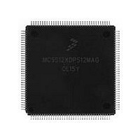
MC9S12XDP512MAG Freescale, MC9S12XDP512MAG Datasheet - Page 1253

MC9S12XDP512MAG
Manufacturer Part Number
MC9S12XDP512MAG
Description
Manufacturer
Freescale
Datasheet
1.MC9S12XDP512MAG.pdf
(1348 pages)
Specifications of MC9S12XDP512MAG
Cpu Family
HCS12
Device Core Size
16b
Frequency (max)
40MHz
Interface Type
CAN/I2C/SCI/SPI
Total Internal Ram Size
32KB
# I/os (max)
119
Number Of Timers - General Purpose
12
Operating Supply Voltage (typ)
2.5/5V
Operating Supply Voltage (max)
2.75/5.5V
Operating Supply Voltage (min)
2.35/3.15V
On-chip Adc
2(24-chx10-bit)
Instruction Set Architecture
CISC
Operating Temp Range
-40C to 125C
Operating Temperature Classification
Automotive
Mounting
Surface Mount
Pin Count
144
Package Type
LQFP
Program Memory Type
Flash
Program Memory Size
512KB
Lead Free Status / RoHS Status
Compliant
Available stocks
Company
Part Number
Manufacturer
Quantity
Price
Company:
Part Number:
MC9S12XDP512MAG
Manufacturer:
FREESCALE
Quantity:
5 530
Company:
Part Number:
MC9S12XDP512MAG
Manufacturer:
Exar
Quantity:
20
Company:
Part Number:
MC9S12XDP512MAG
Manufacturer:
Freescale Semiconductor
Quantity:
10 000
- Current page: 1253 of 1348
- Download datasheet (8Mb)
A.2.2.3
There are two cases to consider.
1
Freescale Semiconductor
Conditions are shown in
Num C
See also Table A-7. item 14
1
2
3
4
5
1. A current is injected into the channel being converted. The channel being stressed has conversion
2. Current is injected into pins in the neighborhood of the channel being converted. A portion of this
C Max input source resistance
C Disruptive analog input current
C Coupling ratio positive current injection
C Coupling ratio negative current injection
T Total input capacitance
values of $3FF ($FF in 8-bit mode) for analog inputs greater than V
than V
current is picked up by the channel (coupling ratio K), This additional current impacts the accuracy
of the conversion depending on the source resistance.
The additional input voltage error on the converted channel can be calculated as:
with I
Non sampling
Sampling
INJ
Current Injection
RL
V
being the sum of the currents injected into the two pins adjacent to the converted channel.
ERR
unless the current is higher than specified as disruptive condition.
Table A-4
= K * R
S
unless otherwise noted
Rating
* I
Table A-14. ATD Electrical Characteristics
INJ
1
MC9S12XDP512 Data Sheet, Rev. 2.21
Symbol
C
C
I
R
K
K
NA
INN
INS
S
p
n
–2.5
Min
—
—
—
—
—
Appendix A Electrical Characteristics
RH
and $000 for values less
Typ
—
—
—
—
—
—
Max
10
10
2.5
10
22
1
-4
-2
Unit
A/A
A/A
mA
K
pF
1255
Related parts for MC9S12XDP512MAG
Image
Part Number
Description
Manufacturer
Datasheet
Request
R

Part Number:
Description:
16-BIT MICROPROCESSOR FAMILY
Manufacturer:
FREESCALE [Freescale Semiconductor, Inc]
Datasheet:

Part Number:
Description:
TOWER ELEVATOR BOARDS HARDWARE
Manufacturer:
Freescale Semiconductor
Datasheet:

Part Number:
Description:
TOWER SERIAL I/O HARDWARE
Manufacturer:
Freescale Semiconductor
Datasheet:

Part Number:
Description:
LCD MODULE FOR TWR SYSTEM
Manufacturer:
Freescale Semiconductor
Datasheet:

Part Number:
Description:
DAUGHTER LCD WVGA I.MX51
Manufacturer:
Freescale Semiconductor
Datasheet:

Part Number:
Description:
TOWER SYSTEM BOARD MPC5125
Manufacturer:
Freescale Semiconductor
Datasheet:

Part Number:
Description:
KIT EVALUATION I.MX51
Manufacturer:
Freescale Semiconductor
Datasheet:

Part Number:
Description:
KIT DEVELOPMENT WINCE IMX25
Manufacturer:
Freescale Semiconductor
Datasheet:

Part Number:
Description:
TOWER SYSTEM KIT MPC5125
Manufacturer:
Freescale Semiconductor
Datasheet:

Part Number:
Description:
TOWER SYSTEM BOARD K40X256
Manufacturer:
Freescale Semiconductor
Datasheet:

Part Number:
Description:
TOWER SYSTEM KIT K40X256
Manufacturer:
Freescale Semiconductor
Datasheet:

Part Number:
Description:
Microcontrollers (MCU) MX28 PLATFORM DEV KIT
Manufacturer:
Freescale Semiconductor
Datasheet:

Part Number:
Description:
MCU, MPU & DSP Development Tools IAR KickStart Kit for Kinetis K60
Manufacturer:
Freescale Semiconductor
Datasheet:

Part Number:
Description:
24BIT HDMI MX535/08
Manufacturer:
Freescale Semiconductor
Datasheet:
Part Number:
Description:
Manufacturer:
Freescale Semiconductor, Inc
Datasheet:


