MC9S12XDP512MAG Freescale, MC9S12XDP512MAG Datasheet - Page 368
MC9S12XDP512MAG
Manufacturer Part Number
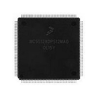
MC9S12XDP512MAG
Description
Manufacturer
Freescale
Datasheet
1.MC9S12XDP512MAG.pdf
(1348 pages)
Specifications of MC9S12XDP512MAG
Cpu Family
HCS12
Device Core Size
16b
Frequency (max)
40MHz
Interface Type
CAN/I2C/SCI/SPI
Total Internal Ram Size
32KB
# I/os (max)
119
Number Of Timers - General Purpose
12
Operating Supply Voltage (typ)
2.5/5V
Operating Supply Voltage (max)
2.75/5.5V
Operating Supply Voltage (min)
2.35/3.15V
On-chip Adc
2(24-chx10-bit)
Instruction Set Architecture
CISC
Operating Temp Range
-40C to 125C
Operating Temperature Classification
Automotive
Mounting
Surface Mount
Pin Count
144
Package Type
LQFP
Program Memory Type
Flash
Program Memory Size
512KB
Lead Free Status / RoHS Status
Compliant
Available stocks
Company
Part Number
Manufacturer
Quantity
Price
Company:

Part Number:
MC9S12XDP512MAG
Manufacturer:
FREESCALE
Quantity:
5 530
Company:
Part Number:
MC9S12XDP512MAG
Manufacturer:
Exar
Quantity:
20
Company:
Part Number:
MC9S12XDP512MAG
Manufacturer:
Freescale Semiconductor
Quantity:
10 000


Chapter 8 Pulse-Width Modulator (S12PWM8B8CV1)
1
8.3.2.1
Each PWM channel has an enable bit (PWMEx) to start its waveform output. When any of the PWMEx
bits are set (PWMEx = 1), the associated PWM output is enabled immediately. However, the actual PWM
waveform is not available on the associated PWM output until its clock source begins its next cycle due to
the synchronization of PWMEx and the clock source.
An exception to this is when channels are concatenated. Once concatenated mode is enabled (CONxx bits
set in PWMCTL register), enabling/disabling the corresponding 16-bit PWM channel is controlled by the
368
PWMPER7
PWMDTY0
PWMDTY1
PWMDTY2
PWMDTY3
PWMDTY4
PWMDTY5
PWMDTY6
PWMDTY7
PWMSDN
Intended for factory test purposes only.
Register
Name
W
W
W
W
W
W
W
W
W
W
R
R
R
R
R
R
R
R
R
R
PWM Enable Register (PWME)
The first PWM cycle after enabling the channel can be irregular.
PWMIF
Bit 7
Bit 7
Bit 7
Bit 7
Bit 7
Bit 7
Bit 7
Bit 7
Bit 7
Bit 7
= Unimplemented or Reserved
Figure 8-2. PWM Register Summary (Sheet 3 of 3)
PWMIE
6
6
6
6
6
6
6
6
6
6
MC9S12XDP512 Data Sheet, Rev. 2.21
PWMRSTRT
5
0
5
5
5
5
5
5
5
5
5
NOTE
PWMLVL
4
4
4
4
4
4
4
4
4
4
3
0
3
3
3
3
3
3
3
3
3
PWM7IN
2
2
2
2
2
2
2
2
2
2
PWM7INL
Freescale Semiconductor
1
1
1
1
1
1
1
1
1
1
PWM7ENA
Bit 0
Bit 0
Bit 0
Bit 0
Bit 0
Bit 0
Bit 0
Bit 0
Bit 0
Bit 0
Related parts for MC9S12XDP512MAG
Image
Part Number
Description
Manufacturer
Datasheet
Request
R

Part Number:
Description:
16-BIT MICROPROCESSOR FAMILY
Manufacturer:
FREESCALE [Freescale Semiconductor, Inc]
Datasheet:

Part Number:
Description:
TOWER ELEVATOR BOARDS HARDWARE
Manufacturer:
Freescale Semiconductor
Datasheet:

Part Number:
Description:
TOWER SERIAL I/O HARDWARE
Manufacturer:
Freescale Semiconductor
Datasheet:

Part Number:
Description:
LCD MODULE FOR TWR SYSTEM
Manufacturer:
Freescale Semiconductor
Datasheet:

Part Number:
Description:
DAUGHTER LCD WVGA I.MX51
Manufacturer:
Freescale Semiconductor
Datasheet:

Part Number:
Description:
TOWER SYSTEM BOARD MPC5125
Manufacturer:
Freescale Semiconductor
Datasheet:

Part Number:
Description:
KIT EVALUATION I.MX51
Manufacturer:
Freescale Semiconductor
Datasheet:

Part Number:
Description:
KIT DEVELOPMENT WINCE IMX25
Manufacturer:
Freescale Semiconductor
Datasheet:

Part Number:
Description:
TOWER SYSTEM KIT MPC5125
Manufacturer:
Freescale Semiconductor
Datasheet:

Part Number:
Description:
TOWER SYSTEM BOARD K40X256
Manufacturer:
Freescale Semiconductor
Datasheet:

Part Number:
Description:
TOWER SYSTEM KIT K40X256
Manufacturer:
Freescale Semiconductor
Datasheet:

Part Number:
Description:
Microcontrollers (MCU) MX28 PLATFORM DEV KIT
Manufacturer:
Freescale Semiconductor
Datasheet:

Part Number:
Description:
MCU, MPU & DSP Development Tools IAR KickStart Kit for Kinetis K60
Manufacturer:
Freescale Semiconductor
Datasheet:

Part Number:
Description:
24BIT HDMI MX535/08
Manufacturer:
Freescale Semiconductor
Datasheet:

Part Number:
Description:
Manufacturer:
Freescale Semiconductor, Inc
Datasheet: