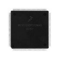
MC9S12XDP512MAG Freescale, MC9S12XDP512MAG Datasheet - Page 189

MC9S12XDP512MAG
Manufacturer Part Number
MC9S12XDP512MAG
Description
Manufacturer
Freescale
Datasheet
1.MC9S12XDP512MAG.pdf
(1348 pages)
Specifications of MC9S12XDP512MAG
Cpu Family
HCS12
Device Core Size
16b
Frequency (max)
40MHz
Interface Type
CAN/I2C/SCI/SPI
Total Internal Ram Size
32KB
# I/os (max)
119
Number Of Timers - General Purpose
12
Operating Supply Voltage (typ)
2.5/5V
Operating Supply Voltage (max)
2.75/5.5V
Operating Supply Voltage (min)
2.35/3.15V
On-chip Adc
2(24-chx10-bit)
Instruction Set Architecture
CISC
Operating Temp Range
-40C to 125C
Operating Temperature Classification
Automotive
Mounting
Surface Mount
Pin Count
144
Package Type
LQFP
Program Memory Type
Flash
Program Memory Size
512KB
Lead Free Status / RoHS Status
Compliant
Available stocks
Company
Part Number
Manufacturer
Quantity
Price
Company:
Part Number:
MC9S12XDP512MAG
Manufacturer:
FREESCALE
Quantity:
5 530
Company:
Part Number:
MC9S12XDP512MAG
Manufacturer:
Exar
Quantity:
20
Company:
Part Number:
MC9S12XDP512MAG
Manufacturer:
Freescale Semiconductor
Quantity:
10 000
- Current page: 189 of 1348
- Download datasheet (8Mb)
6.3.1.1
All module level switches and flags are located in the module control register
Read: Anytime
Write: Anytime
Freescale Semiconductor
Reset
XGDBGM
XGFRZM
XGSSM
XGEM
Field
W
R
15
14
13
12
XGEM
15
0
0
XGE Mask — This bit controls the write access to the XGE bit. The XGE bit can only be set or cleared if a "1" is
written to the XGEM bit in the same register access.
Read:
Write:
0 Disable write access to the XGE in the same bus cycle
1 Enable write access to the XGE in the same bus cycle
XGFRZ Mask — This bit controls the write access to the XGFRZ bit. The XGFRZ bit can only be set or cleared
if a "1" is written to the XGFRZM bit in the same register access.
Read:
Write:
0 Disable write access to the XGFRZ in the same bus cycle
1 Enable write access to the XGFRZ in the same bus cycle
XGDBG Mask — This bit controls the write access to the XGDBG bit. The XGDBG bit can only be set or cleared
if a "1" is written to the XGDBGM bit in the same register access.
Read:
Write:
0 Disable write access to the XGDBG in the same bus cycle
1 Enable write access to the XGDBG in the same bus cycle
XGSS Mask — This bit controls the write access to the XGSS bit. The XGSS bit can only be set or cleared if a
"1" is written to the XGSSM bit in the same register access.
Read:
Write:
0 Disable write access to the XGSS in the same bus cycle
1 Enable write access to the XGSS in the same bus cycle
FRZM
XGATE Control Register (XGMCTL)
XG
14
0
0
This bit will always read "0".
This bit will always read "0".
This bit will always read "0".
This bit will always read "0".
= Unimplemented or Reserved
DBGM
XG
13
0
0
SSM
XG
12
Table 6-1. XGMCTL Field Descriptions (Sheet 1 of 3)
0
0
Figure 6-3. XGATE Control Register (XGMCTL)
FACTM
XG
11
0
0
MC9S12XDP512 Data Sheet, Rev. 2.21
10
0
0
SWEIFM
XG
0
0
9
XGIEM
0
0
8
Description
XGE XGFRZ XGDBG XGSS XGFACT
7
0
0
6
0
5
0
4
Figure
Chapter 6 XGATE (S12XGATEV2)
0
3
6-3.
2
0
0
SWEIF
XG
0
1
XGIE
0
0
189
Related parts for MC9S12XDP512MAG
Image
Part Number
Description
Manufacturer
Datasheet
Request
R

Part Number:
Description:
16-BIT MICROPROCESSOR FAMILY
Manufacturer:
FREESCALE [Freescale Semiconductor, Inc]
Datasheet:

Part Number:
Description:
TOWER ELEVATOR BOARDS HARDWARE
Manufacturer:
Freescale Semiconductor
Datasheet:

Part Number:
Description:
TOWER SERIAL I/O HARDWARE
Manufacturer:
Freescale Semiconductor
Datasheet:

Part Number:
Description:
LCD MODULE FOR TWR SYSTEM
Manufacturer:
Freescale Semiconductor
Datasheet:

Part Number:
Description:
DAUGHTER LCD WVGA I.MX51
Manufacturer:
Freescale Semiconductor
Datasheet:

Part Number:
Description:
TOWER SYSTEM BOARD MPC5125
Manufacturer:
Freescale Semiconductor
Datasheet:

Part Number:
Description:
KIT EVALUATION I.MX51
Manufacturer:
Freescale Semiconductor
Datasheet:

Part Number:
Description:
KIT DEVELOPMENT WINCE IMX25
Manufacturer:
Freescale Semiconductor
Datasheet:

Part Number:
Description:
TOWER SYSTEM KIT MPC5125
Manufacturer:
Freescale Semiconductor
Datasheet:

Part Number:
Description:
TOWER SYSTEM BOARD K40X256
Manufacturer:
Freescale Semiconductor
Datasheet:

Part Number:
Description:
TOWER SYSTEM KIT K40X256
Manufacturer:
Freescale Semiconductor
Datasheet:

Part Number:
Description:
Microcontrollers (MCU) MX28 PLATFORM DEV KIT
Manufacturer:
Freescale Semiconductor
Datasheet:

Part Number:
Description:
MCU, MPU & DSP Development Tools IAR KickStart Kit for Kinetis K60
Manufacturer:
Freescale Semiconductor
Datasheet:

Part Number:
Description:
24BIT HDMI MX535/08
Manufacturer:
Freescale Semiconductor
Datasheet:
Part Number:
Description:
Manufacturer:
Freescale Semiconductor, Inc
Datasheet:


