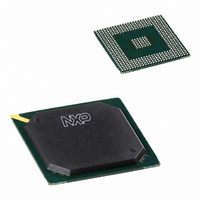
PNX1500E/G,557 NXP Semiconductors, PNX1500E/G,557 Datasheet - Page 209

PNX1500E/G,557
Manufacturer Part Number
PNX1500E/G,557
Description
IC MEDIA PROC 240MHZ 456-BGA
Manufacturer
NXP Semiconductors
Specifications of PNX1500E/G,557
Applications
Multimedia
Core Processor
TriMedia
Controller Series
Nexperia
Interface
I²C, 2-Wire Serial
Number Of I /o
61
Voltage - Supply
1.14 V ~ 1.26 V
Operating Temperature
0°C ~ 85°C
Mounting Type
Surface Mount
Package / Case
456-BGA
Lead Free Status / RoHS Status
Lead free / RoHS Compliant
Program Memory Type
-
Ram Size
-
Lead Free Status / Rohs Status
Compliant
Other names
568-1296
935277746557
PNX1500E/G
935277746557
PNX1500E/G
- Current page: 209 of 828
- Download datasheet (8Mb)
Philips Semiconductors
Volume 1 of 1
Table 2: The Boot Commands
3. PNX15xx Series Boot Scripts Content
PNX15XX_SER_3
Product data sheet
Command
write(address,value)
writelist(a,lenght,valarray)
delay(ncycles)
Terminate Boot
3.1 The Common Behavior
Encoding (32 bits each)
Address:
aaaaaaaaaaaaaaaaaaaaaaaaaaaaaa00
Value:
vvvvvvvvvvvvvvvvvvvvvvvvvvvvvvv
Address:
aaaaaaaaaaaaaaaaaaaaaaaaaaaaaa01
length<n>:
nnnnnnnnnnnnnnnnnnnnnnnnnnnnn
value<1>:
vvvvvvvvvvvvvvvvvvvvvvvvvvvvvvv
value<2>:
vvvvvvvvvvvvvvvvvvvvvvvvvvvvvvv
.
.
value<n>:
vvvvvvvvvvvvvvvvvvvvvvvvvvvvvvv
nnnnnnnnnnnnnnnnnnnnnnnnnnnn0010
nnnnnnnnnnnnnnnnnnnnnnnnnnnn0110
xxxxxxxxxxxxxxxxxxxxxxxxxxxx1x1x
The following
Unlike PNX1300 Series systems [1], PNX15xx Series uses internal boot scripts to
provide some cost savings at board level by allowing the building of products without
the need of an external EEPROM. The following sections describes the content of
these scripts. If the content of these internal boot scripts is not suitable for the
PNX15xx Series based product, then an EEPROM should be used to override the
internal boot scripts, see
The three scripts have a common section which is the initial configuration sequence
of the PNX15xx Series system. The differences between the boot scripts is detailed
in the next sections. The common behavior is described bellow in the order in which it
happens:
1. Enable the clocks for the TM3260, 100 MHz, and the MMI, 125 MHz, modules.
2. Enable the clocks for the MMIO bus (a.k.a. the DCS Bus), 102 MHz, and the
PCI_SYS_CLK, 33.23 MHz, clocks.
Table 2
Rev. 3 — 17 March 2006
documents the coding of the four commands.
Section
4..
Description
Write a single 32-bit value, ‘V’ at address ‘A’ (32-bit
word aligned) MMIO bus or memory address.
‘A’ is the 30-bit value composed by the <a...a> bits
concatenated with two 0s (makes it a 32-bit word
address).
‘V’ is the 32-bit value composed by the <v...v> bits.
Write an arbitrary length list of 32-bit values,
value<1>,..., value<n>, starting at address ‘A’ (32-
bit aligned) MMIO bus or memory address.
value<1> is written at address ‘A’ + 0, value<n> is
written at the 32-bit word address ‘A+n-1’.
‘A’ is the 30-bit value composed by the <a...a> bits
concatenated with two 0s (makes it a 32-bit word
address).
Delay by N 27 MHz cycle periods.
Where N is the 28-bit value composed by the
<n...n> bits.
End boot process. The Boot module releases I2C
bus and becomes non-active until a hardware reset
or software reset occurs.
Reserved for future use.
© Koninklijke Philips Electronics N.V. 2006. All rights reserved.
PNX15xx Series
Chapter 6: Boot Module
6-6
Related parts for PNX1500E/G,557
Image
Part Number
Description
Manufacturer
Datasheet
Request
R

Part Number:
Description:
Manufacturer:
NXP Semiconductors
Datasheet:
Part Number:
Description:
Digital Signal Processors & Controllers - DSP, DSC NEXPERIA MEDIA PROC 240MHZ
Manufacturer:
NXP Semiconductors
Part Number:
Description:
Digital Signal Processors & Controllers - DSP, DSC PNX1500, 240MHZ
Manufacturer:
NXP Semiconductors
Part Number:
Description:
NXP Semiconductors designed the LPC2420/2460 microcontroller around a 16-bit/32-bitARM7TDMI-S CPU core with real-time debug interfaces that include both JTAG andembedded trace
Manufacturer:
NXP Semiconductors
Datasheet:

Part Number:
Description:
NXP Semiconductors designed the LPC2458 microcontroller around a 16-bit/32-bitARM7TDMI-S CPU core with real-time debug interfaces that include both JTAG andembedded trace
Manufacturer:
NXP Semiconductors
Datasheet:
Part Number:
Description:
NXP Semiconductors designed the LPC2468 microcontroller around a 16-bit/32-bitARM7TDMI-S CPU core with real-time debug interfaces that include both JTAG andembedded trace
Manufacturer:
NXP Semiconductors
Datasheet:
Part Number:
Description:
NXP Semiconductors designed the LPC2470 microcontroller, powered by theARM7TDMI-S core, to be a highly integrated microcontroller for a wide range ofapplications that require advanced communications and high quality graphic displays
Manufacturer:
NXP Semiconductors
Datasheet:
Part Number:
Description:
NXP Semiconductors designed the LPC2478 microcontroller, powered by theARM7TDMI-S core, to be a highly integrated microcontroller for a wide range ofapplications that require advanced communications and high quality graphic displays
Manufacturer:
NXP Semiconductors
Datasheet:
Part Number:
Description:
The Philips Semiconductors XA (eXtended Architecture) family of 16-bit single-chip microcontrollers is powerful enough to easily handle the requirements of high performance embedded applications, yet inexpensive enough to compete in the market for hi
Manufacturer:
NXP Semiconductors
Datasheet:
Part Number:
Description:
The XA-S3 device is a member of Philips Semiconductors? XA(eXtended Architecture) family of high performance 16-bitsingle-chip microcontrollers
Manufacturer:
NXP Semiconductors
Datasheet:

Part Number:
Description:
The NXP BlueStreak LH75401/LH75411 family consists of two low-cost 16/32-bit System-on-Chip (SoC) devices
Manufacturer:
NXP Semiconductors
Datasheet:

Part Number:
Description:
The NXP LPC3130/3131 combine an 180 MHz ARM926EJ-S CPU core, high-speed USB2
Manufacturer:
NXP Semiconductors
Datasheet:

Part Number:
Description:
The NXP LPC3141 combine a 270 MHz ARM926EJ-S CPU core, High-speed USB 2
Manufacturer:
NXP Semiconductors

Part Number:
Description:
The NXP LPC3143 combine a 270 MHz ARM926EJ-S CPU core, High-speed USB 2
Manufacturer:
NXP Semiconductors


