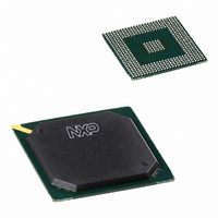
PNX1500E/G,557 NXP Semiconductors, PNX1500E/G,557 Datasheet - Page 755

PNX1500E/G,557
Manufacturer Part Number
PNX1500E/G,557
Description
IC MEDIA PROC 240MHZ 456-BGA
Manufacturer
NXP Semiconductors
Specifications of PNX1500E/G,557
Applications
Multimedia
Core Processor
TriMedia
Controller Series
Nexperia
Interface
I²C, 2-Wire Serial
Number Of I /o
61
Voltage - Supply
1.14 V ~ 1.26 V
Operating Temperature
0°C ~ 85°C
Mounting Type
Surface Mount
Package / Case
456-BGA
Lead Free Status / RoHS Status
Lead free / RoHS Compliant
Program Memory Type
-
Ram Size
-
Lead Free Status / Rohs Status
Compliant
Other names
568-1296
935277746557
PNX1500E/G
935277746557
PNX1500E/G
- Current page: 755 of 828
- Download datasheet (8Mb)
Philips Semiconductors
Volume 1 of 1
PNX15XX_SER_3
Product data sheet
4.1 Register Summary
JTAG Virtual Registers
There are two virtual registers, TM_DBG_IFULL_IN and TM_DBG_OFULL_OUT:
Table 4: Register Summary
Offset
0x06 1000
0x06 1004
0x06 1008
0x06 100C
0x06 1FE0
0x06 1FE4
0x06 1FE8
0x06 1FEC TM_DBG_N_INT_SET
0x06 1FF0
0x06 1FF4
0x06 1FF8
0x06 1FFC
•
•
•
and writable via JTAG. Writing 0 to TM_DBG_CTRL2.ifull via JTAG is a
‘remember’ operation i.e., TM_DBG_CTRL2.ifull retains it previous state. Writing
1 to TM_DBG_CTRL2.ifull posts a TM3260 interrupt on hardware line 49.
The TM_DBG_CTRL1.sleepless bit has no longer a function. However it still can
be read and written to by the PNX15xx Series CPU via load/store operations and
by the debugger front-end running on a host by scan in/out.
The first virtual register TM_DBG_IFULL_IN connects the registers
TM_DBG_CTRL2.ifull and TM_DBG_DATA_IN in series. Likewise, the virtual
register TM_DBG_OFULL_OUT connects TM_DBG_CTRL1.ofull and
TM_DBG_DATA_OUT in series.
The reason for the virtual registers is to shorten the time for scanning the
TM_DBG_DATA_IN and TM_DBG_DATA_OUT registers. Without virtual
registers, one must scan in an instruction to select TM_DBG_DATA_IN, scan in
data, scan an instruction to select TM_DBG_CTRL register and finally scan in the
control register. With virtual register, one can scan in an instruction to select
TM_DBG_IFULL_IN and then scan in both control and data bits. Similar savings
can be achieved for scan out using virtual registers.
Symbol
TM_DBG_N_DATA_IN
TM_DBG_N_DATA_OUT
TM_DBG_N_CTRL1
TM_DBG_N_CTRL2
TM_DBG_N_INT_ST
TM_DBG_N_INT_EN
TM_DBG_N_INT_CLR
Reserved
TM_DBG_N_POWER_DOWN
Reserved
Module ID
Rev. 3 — 17 March 2006
Description
Input register for data coming from the JTAG
Output register for data going to the JTAG
Control register 1 for output data
Control register 2 for input data
Interrupt Status Register
Interrupt Enable Register
Interrupt Clear Register
Interrupt Set Register
Powerdown Register
Module Identification Register
© Koninklijke Philips Electronics N.V. 2006. All rights reserved.
Chapter 24: TM3260 Debug
PNX15xx Series
24-9
Related parts for PNX1500E/G,557
Image
Part Number
Description
Manufacturer
Datasheet
Request
R

Part Number:
Description:
Manufacturer:
NXP Semiconductors
Datasheet:
Part Number:
Description:
Digital Signal Processors & Controllers - DSP, DSC NEXPERIA MEDIA PROC 240MHZ
Manufacturer:
NXP Semiconductors
Part Number:
Description:
Digital Signal Processors & Controllers - DSP, DSC PNX1500, 240MHZ
Manufacturer:
NXP Semiconductors
Part Number:
Description:
NXP Semiconductors designed the LPC2420/2460 microcontroller around a 16-bit/32-bitARM7TDMI-S CPU core with real-time debug interfaces that include both JTAG andembedded trace
Manufacturer:
NXP Semiconductors
Datasheet:

Part Number:
Description:
NXP Semiconductors designed the LPC2458 microcontroller around a 16-bit/32-bitARM7TDMI-S CPU core with real-time debug interfaces that include both JTAG andembedded trace
Manufacturer:
NXP Semiconductors
Datasheet:
Part Number:
Description:
NXP Semiconductors designed the LPC2468 microcontroller around a 16-bit/32-bitARM7TDMI-S CPU core with real-time debug interfaces that include both JTAG andembedded trace
Manufacturer:
NXP Semiconductors
Datasheet:
Part Number:
Description:
NXP Semiconductors designed the LPC2470 microcontroller, powered by theARM7TDMI-S core, to be a highly integrated microcontroller for a wide range ofapplications that require advanced communications and high quality graphic displays
Manufacturer:
NXP Semiconductors
Datasheet:
Part Number:
Description:
NXP Semiconductors designed the LPC2478 microcontroller, powered by theARM7TDMI-S core, to be a highly integrated microcontroller for a wide range ofapplications that require advanced communications and high quality graphic displays
Manufacturer:
NXP Semiconductors
Datasheet:
Part Number:
Description:
The Philips Semiconductors XA (eXtended Architecture) family of 16-bit single-chip microcontrollers is powerful enough to easily handle the requirements of high performance embedded applications, yet inexpensive enough to compete in the market for hi
Manufacturer:
NXP Semiconductors
Datasheet:
Part Number:
Description:
The XA-S3 device is a member of Philips Semiconductors? XA(eXtended Architecture) family of high performance 16-bitsingle-chip microcontrollers
Manufacturer:
NXP Semiconductors
Datasheet:

Part Number:
Description:
The NXP BlueStreak LH75401/LH75411 family consists of two low-cost 16/32-bit System-on-Chip (SoC) devices
Manufacturer:
NXP Semiconductors
Datasheet:

Part Number:
Description:
The NXP LPC3130/3131 combine an 180 MHz ARM926EJ-S CPU core, high-speed USB2
Manufacturer:
NXP Semiconductors
Datasheet:

Part Number:
Description:
The NXP LPC3141 combine a 270 MHz ARM926EJ-S CPU core, High-speed USB 2
Manufacturer:
NXP Semiconductors

Part Number:
Description:
The NXP LPC3143 combine a 270 MHz ARM926EJ-S CPU core, High-speed USB 2
Manufacturer:
NXP Semiconductors


