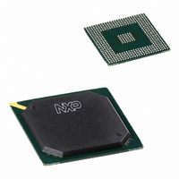
PNX1500E/G,557 NXP Semiconductors, PNX1500E/G,557 Datasheet - Page 563

PNX1500E/G,557
Manufacturer Part Number
PNX1500E/G,557
Description
IC MEDIA PROC 240MHZ 456-BGA
Manufacturer
NXP Semiconductors
Specifications of PNX1500E/G,557
Applications
Multimedia
Core Processor
TriMedia
Controller Series
Nexperia
Interface
I²C, 2-Wire Serial
Number Of I /o
61
Voltage - Supply
1.14 V ~ 1.26 V
Operating Temperature
0°C ~ 85°C
Mounting Type
Surface Mount
Package / Case
456-BGA
Lead Free Status / RoHS Status
Lead free / RoHS Compliant
Program Memory Type
-
Ram Size
-
Lead Free Status / Rohs Status
Compliant
Other names
568-1296
935277746557
PNX1500E/G
935277746557
PNX1500E/G
- Current page: 563 of 828
- Download datasheet (8Mb)
Philips Semiconductors
Volume 1 of 1
PNX15XX_SER_3
Product data sheet
3.1.4 SPDIF Input and the Oversampling Clock
3.2.1 SPDIF Input Register Set
3.2 Register Programming Guidelines
or 0.26UI pk-pk (1 UI = 1/128 Fs ). For a particular Fs , the max jitter is shown in
Table
Table 2: Input Jitter for Different Sample Rates
The SPDIF Input receiver will reproduce the input data and clock without error if the
maximum input jitter remains within the specified max jitter tolerance above. The
receiver design meets and exceeds the IEC60958-3 consumer jitter requirements
specification (i.e 0.25 UI pk-pk between 200 Hz and 400 kHz jitter freq. ).
The oversampling clock supplied to the input receiver is derived from a divider in the
central clock control block. The divider value to select is determined by
the oversampling clock has been selected by programming a divider value, the
condition of the LOCK bit status indicator in SPDI_STATUS provides feedback on
whether the selected oversampling clock has allowed the interface to achieve lock
onto the incoming SPDIF input stream. The settings provided by the divider for the
oversampling clock are sufficient for capture of 32 kHz, 44.1 kHz, 48 kHz and 96 kHz
sample rate input streams.
The S/PDIF register set is outlined in
page
to configure SPDIF Input data capture and DMA of audio data to main memory. To
ensure compatibility with future devices, any reserved MMIO register bits in
and
Fs (kHz)
32
44.1
48
96
Figure 6:
Figure 10
SPDI_IN
18-16. The register set is composed of status and control functions necessary
2.
SPDIF Input domain
Central clocking domain
PIN
SPDIF Input Oversampling Clock Generation
should be ignored when read, and written as zeroes .
Rev. 3 — 17 March 2006
1 UI = 1/(128 Fs) (nsec)
244.1
177.2
162.8
81.4
SPDIF Input
Receiver
oversampling
clock
Figure 9 on page 18-15
Divide by n
n = 3, 6
SPDIF Input
Decoder
Max Jitter = 0.26UI pk-pk (nsec)
31.7
23.0
21.2
10.6
432MHz (16x27MHz)
© Koninklijke Philips Electronics N.V. 2006. All rights reserved.
PNX15xx Series
Chapter 18: SPDIF Input
and
Figure 10 on
Memory Bound
Audio Data
Table
Figure 9
1. Once
18-7
Related parts for PNX1500E/G,557
Image
Part Number
Description
Manufacturer
Datasheet
Request
R

Part Number:
Description:
Manufacturer:
NXP Semiconductors
Datasheet:
Part Number:
Description:
Digital Signal Processors & Controllers - DSP, DSC NEXPERIA MEDIA PROC 240MHZ
Manufacturer:
NXP Semiconductors
Part Number:
Description:
Digital Signal Processors & Controllers - DSP, DSC PNX1500, 240MHZ
Manufacturer:
NXP Semiconductors
Part Number:
Description:
NXP Semiconductors designed the LPC2420/2460 microcontroller around a 16-bit/32-bitARM7TDMI-S CPU core with real-time debug interfaces that include both JTAG andembedded trace
Manufacturer:
NXP Semiconductors
Datasheet:

Part Number:
Description:
NXP Semiconductors designed the LPC2458 microcontroller around a 16-bit/32-bitARM7TDMI-S CPU core with real-time debug interfaces that include both JTAG andembedded trace
Manufacturer:
NXP Semiconductors
Datasheet:
Part Number:
Description:
NXP Semiconductors designed the LPC2468 microcontroller around a 16-bit/32-bitARM7TDMI-S CPU core with real-time debug interfaces that include both JTAG andembedded trace
Manufacturer:
NXP Semiconductors
Datasheet:
Part Number:
Description:
NXP Semiconductors designed the LPC2470 microcontroller, powered by theARM7TDMI-S core, to be a highly integrated microcontroller for a wide range ofapplications that require advanced communications and high quality graphic displays
Manufacturer:
NXP Semiconductors
Datasheet:
Part Number:
Description:
NXP Semiconductors designed the LPC2478 microcontroller, powered by theARM7TDMI-S core, to be a highly integrated microcontroller for a wide range ofapplications that require advanced communications and high quality graphic displays
Manufacturer:
NXP Semiconductors
Datasheet:
Part Number:
Description:
The Philips Semiconductors XA (eXtended Architecture) family of 16-bit single-chip microcontrollers is powerful enough to easily handle the requirements of high performance embedded applications, yet inexpensive enough to compete in the market for hi
Manufacturer:
NXP Semiconductors
Datasheet:
Part Number:
Description:
The XA-S3 device is a member of Philips Semiconductors? XA(eXtended Architecture) family of high performance 16-bitsingle-chip microcontrollers
Manufacturer:
NXP Semiconductors
Datasheet:

Part Number:
Description:
The NXP BlueStreak LH75401/LH75411 family consists of two low-cost 16/32-bit System-on-Chip (SoC) devices
Manufacturer:
NXP Semiconductors
Datasheet:

Part Number:
Description:
The NXP LPC3130/3131 combine an 180 MHz ARM926EJ-S CPU core, high-speed USB2
Manufacturer:
NXP Semiconductors
Datasheet:

Part Number:
Description:
The NXP LPC3141 combine a 270 MHz ARM926EJ-S CPU core, High-speed USB 2
Manufacturer:
NXP Semiconductors

Part Number:
Description:
The NXP LPC3143 combine a 270 MHz ARM926EJ-S CPU core, High-speed USB 2
Manufacturer:
NXP Semiconductors


