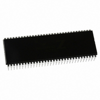
Z8018010PSG Zilog, Z8018010PSG Datasheet - Page 22

Z8018010PSG
Manufacturer Part Number
Z8018010PSG
Description
IC 10MHZ Z180 CMOS ENH MPU 64DIP
Manufacturer
Zilog
Specifications of Z8018010PSG
Processor Type
Z180
Features
8-Bit, Enhanced Z80 Megacell
Speed
10MHz
Voltage
5V
Mounting Type
Through Hole
Package / Case
64-DIP (0.750", 19.05mm)
Processor Series
Z8018xx
Core
Z80
Data Bus Width
8 bit
Maximum Clock Frequency
10 MHz
Number Of Timers
2
Operating Supply Voltage
0 V to 5 V
Maximum Operating Temperature
+ 70 C
Mounting Style
Through Hole
Minimum Operating Temperature
0 C
Core Size
8bit
Cpu Speed
10MHz
Digital Ic Case Style
DIP
No. Of Pins
64
Supply Voltage Range
4.5V To 5.5V
Operating Temperature Range
0°C To +70°C
Svhc
No SVHC (18-Jun-2010)
Base Number
8018010
Rohs Compliant
Yes
Clock Frequency
10MHz
Lead Free Status / RoHS Status
Lead free / RoHS Compliant
Other names
269-3889
Z8018010PSG
Z8018010PSG
Available stocks
Company
Part Number
Manufacturer
Quantity
Price
Company:
Part Number:
Z8018010PSG
Manufacturer:
Zilog
Quantity:
40
- Current page: 22 of 326
- Download datasheet (5Mb)
Z8018x
Family MPU User Manual
7
PIN DESCRIPTION
A0–A19. Address Bus (Output, Active High, 3-state). A0–A19 form a 20-
bit address bus. The Address Bus provides the address for memory data
bus exchanges, up to 1 MB, and I/O data bus exchanges, up to 64K. The
address bus enters a high impedance state during RESET and external bus
acknowledge cycles. Address line A18 is multiplexed with the output of
PRT channel 1 (TOUT, selected as address output on RESET) and address
line A19 is not available in DIP versions of the Z8X180.
BUSACK. Bus Acknowledge (Output, Active Low). BUSACK indicates
that the requesting device, the MPU address and data bus, and some
control signals, have entered their high impedance state.
BUSREQ. Bus Request (Input, Active Low). This input is used by
external devices (such as DMA controllers) to request access to the
system bus. This request has a higher priority than NMI and is always
recognized at the end of the current machine cycle. This signal stops the
CPU from executing further instructions and places the address and data
buses, and other control signals, into the high impedance state.
CKA0, CKA1. Asynchronous Clock 0 and 1 (Bidirectional, Active High).
These pins are the transmit and receive clocks for the ASCI channels.
CKA0, is multiplexed with DREQ0 and CKA1 is multiplexed with
TEND0.
CKS. Serial Clock (Bidirectional, Active High). This line is the clock for
the CSIO channel.
CLOCK (PHI). System Clock (Output, Active High). The output is used
as a reference clock for the MPU and the external system. The frequency
of this output is equal to one-half that of the crystal or input clock
frequency.
CTS0, CTS1. Clear to Send 0 and 1 (Inputs, Active Low). These lines are
modem control signals for the ASCI channels. CTS1 is multiplexed with RXS.
UM005003-0703
Related parts for Z8018010PSG
Image
Part Number
Description
Manufacturer
Datasheet
Request
R

Part Number:
Description:
Microprocessor Unit
Manufacturer:
ZiLOG Semiconductor
Datasheet:

Part Number:
Description:
Z80180 EMULATOR
Manufacturer:
Zilog
Datasheet:

Part Number:
Description:
Z80180, Z8s180, Z8l180 Mpu Operation
Manufacturer:
ZiLOG Semiconductor
Datasheet:

Part Number:
Description:
Communication Controllers, ZILOG INTELLIGENT PERIPHERAL CONTROLLER (ZIP)
Manufacturer:
Zilog, Inc.
Datasheet:

Part Number:
Description:
KIT DEV FOR Z8 ENCORE 16K TO 64K
Manufacturer:
Zilog
Datasheet:

Part Number:
Description:
KIT DEV Z8 ENCORE XP 28-PIN
Manufacturer:
Zilog
Datasheet:

Part Number:
Description:
DEV KIT FOR Z8 ENCORE 8K/4K
Manufacturer:
Zilog
Datasheet:

Part Number:
Description:
KIT DEV Z8 ENCORE XP 28-PIN
Manufacturer:
Zilog
Datasheet:

Part Number:
Description:
DEV KIT FOR Z8 ENCORE 4K TO 8K
Manufacturer:
Zilog
Datasheet:

Part Number:
Description:
CMOS Z8 microcontroller. ROM 16 Kbytes, RAM 256 bytes, speed 16 MHz, 32 lines I/O, 3.0V to 5.5V
Manufacturer:
Zilog, Inc.
Datasheet:

Part Number:
Description:
Low-cost microcontroller. 512 bytes ROM, 61 bytes RAM, 8 MHz
Manufacturer:
Zilog, Inc.
Datasheet:

Part Number:
Description:
Z8 4K OTP Microcontroller
Manufacturer:
Zilog, Inc.
Datasheet:

Part Number:
Description:
CMOS SUPER8 ROMLESS MCU
Manufacturer:
Zilog, Inc.
Datasheet:

Part Number:
Description:
SL1866 CMOSZ8 OTP Microcontroller
Manufacturer:
Zilog, Inc.
Datasheet:


