Z8018010PSG Zilog, Z8018010PSG Datasheet - Page 33
Z8018010PSG
Manufacturer Part Number
Z8018010PSG
Description
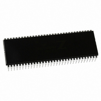
IC 10MHZ Z180 CMOS ENH MPU 64DIP
Manufacturer
Zilog
Specifications of Z8018010PSG
Processor Type
Z180
Features
8-Bit, Enhanced Z80 Megacell
Speed
10MHz
Voltage
5V
Mounting Type
Through Hole
Package / Case
64-DIP (0.750", 19.05mm)
Processor Series
Z8018xx
Core
Z80
Data Bus Width
8 bit
Maximum Clock Frequency
10 MHz
Number Of Timers
2
Operating Supply Voltage
0 V to 5 V
Maximum Operating Temperature
+ 70 C
Mounting Style
Through Hole
Minimum Operating Temperature
0 C
Core Size
8bit
Cpu Speed
10MHz
Digital Ic Case Style
DIP
No. Of Pins
64
Supply Voltage Range
4.5V To 5.5V
Operating Temperature Range
0°C To +70°C
Svhc
No SVHC (18-Jun-2010)
Base Number
8018010
Rohs Compliant
Yes
Clock Frequency
10MHz
Lead Free Status / RoHS Status
Lead free / RoHS Compliant
Other names
269-3889
Z8018010PSG
Z8018010PSG
Available stocks
Company
Part Number
Manufacturer
Quantity
Price
Company:

Part Number:
Z8018010PSG
Manufacturer:
Zilog
Quantity:
40


18
UM005003-0703
Z8018x
Family MPU User Manual
CPU Timing
Note:
This section explains the Z8X180 CPU timing for the following operations:
•
•
•
•
•
•
The basic CPU operation consists of one or more Machine Cycles (MC).
A machine cycle consists of three system clocks, T1, T2, and T3 while
accessing memory or I/O, or it consists of one system clock (T1) during
CPU internal operations. The system clock is half the frequency of the
Crystal oscillator (that is, an 8-MHz crystal produces 4 MHz or 250 nsec).
For interfacing to slow memory or peripherals, optional Wait States (TW)
may be inserted between T2 and T3.
Instruction (Op Code) Fetch Timing
Figure 9 illustrates the instruction (Op Code) fetch timing with no Wait
States. An Op Code fetch cycle is externally indicated when the M1
output pin is Low.
In the first half of T1, the address bus (A0–A19) is driven from the
contents of the Program Counter (PC). This address bus is the translated
address output of the Z8X180 on-chip MMU.
In the second half of T1, the MREQ. (Memory Request) and RD (Read)
signals are asserted Low, enabling the memory.
Instruction (Op Code) fetch timing
Operand and data read/write timing
I/O read/write timing
Basic instruction (fetch and execute) timing
RESET timing
BUSREQ/BUSACK bus exchange timing
The user must program the Operation Mode Control Register
before the first I/O instruction is executed.
Related parts for Z8018010PSG
Image
Part Number
Description
Manufacturer
Datasheet
Request
R

Part Number:
Description:
Microprocessor Unit
Manufacturer:
ZiLOG Semiconductor
Datasheet:

Part Number:
Description:
Z80180 EMULATOR
Manufacturer:
Zilog
Datasheet:
Part Number:
Description:
Z80180, Z8s180, Z8l180 Mpu Operation
Manufacturer:
ZiLOG Semiconductor
Datasheet:

Part Number:
Description:
Communication Controllers, ZILOG INTELLIGENT PERIPHERAL CONTROLLER (ZIP)
Manufacturer:
Zilog, Inc.
Datasheet:

Part Number:
Description:
KIT DEV FOR Z8 ENCORE 16K TO 64K
Manufacturer:
Zilog
Datasheet:

Part Number:
Description:
KIT DEV Z8 ENCORE XP 28-PIN
Manufacturer:
Zilog
Datasheet:

Part Number:
Description:
DEV KIT FOR Z8 ENCORE 8K/4K
Manufacturer:
Zilog
Datasheet:

Part Number:
Description:
KIT DEV Z8 ENCORE XP 28-PIN
Manufacturer:
Zilog
Datasheet:
Part Number:
Description:
DEV KIT FOR Z8 ENCORE 4K TO 8K
Manufacturer:
Zilog
Datasheet:
Part Number:
Description:
CMOS Z8 microcontroller. ROM 16 Kbytes, RAM 256 bytes, speed 16 MHz, 32 lines I/O, 3.0V to 5.5V
Manufacturer:
Zilog, Inc.
Datasheet:
Part Number:
Description:
Low-cost microcontroller. 512 bytes ROM, 61 bytes RAM, 8 MHz
Manufacturer:
Zilog, Inc.
Datasheet:
Part Number:
Description:
Z8 4K OTP Microcontroller
Manufacturer:
Zilog, Inc.
Datasheet:
Part Number:
Description:
CMOS SUPER8 ROMLESS MCU
Manufacturer:
Zilog, Inc.
Datasheet:
Part Number:
Description:
SL1866 CMOSZ8 OTP Microcontroller
Manufacturer:
Zilog, Inc.
Datasheet: