Z8018010PSG Zilog, Z8018010PSG Datasheet - Page 59
Z8018010PSG
Manufacturer Part Number
Z8018010PSG
Description
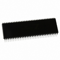
IC 10MHZ Z180 CMOS ENH MPU 64DIP
Manufacturer
Zilog
Specifications of Z8018010PSG
Processor Type
Z180
Features
8-Bit, Enhanced Z80 Megacell
Speed
10MHz
Voltage
5V
Mounting Type
Through Hole
Package / Case
64-DIP (0.750", 19.05mm)
Processor Series
Z8018xx
Core
Z80
Data Bus Width
8 bit
Maximum Clock Frequency
10 MHz
Number Of Timers
2
Operating Supply Voltage
0 V to 5 V
Maximum Operating Temperature
+ 70 C
Mounting Style
Through Hole
Minimum Operating Temperature
0 C
Core Size
8bit
Cpu Speed
10MHz
Digital Ic Case Style
DIP
No. Of Pins
64
Supply Voltage Range
4.5V To 5.5V
Operating Temperature Range
0°C To +70°C
Svhc
No SVHC (18-Jun-2010)
Base Number
8018010
Rohs Compliant
Yes
Clock Frequency
10MHz
Lead Free Status / RoHS Status
Lead free / RoHS Compliant
Other names
269-3889
Z8018010PSG
Z8018010PSG
Available stocks
Company
Part Number
Manufacturer
Quantity
Price
Company:

Part Number:
Z8018010PSG
Manufacturer:
Zilog
Quantity:
40


44
Table 6.
UM005003-0703
ASCI
CSI/O CSI/O Control Register
Z8018x
Family MPU User Manual
Register
ASCI Control Register A Ch 0
ASCI Control Register A Ch 1
ASCI Control Register B Ch 0
ASCI Control Register B Ch 1
ASCI Status Register Ch 0
ASCI Status Register Ch 1
ASCI Transmit Data Register Ch 0
ASCI Transmit Data Register Ch 1
ASCI Receive Data Register Ch 0
ASCI Receive Data Register Ch 1
CSI/O Transmit/Receive Data Register TRD
I/O Address Map for Z80180-Class Processors Only
address to
OTDMR and TSTIO (see Instruction Set).
When writing to an internal I/O register, the same I/O write occurs on the
external bus. However, the duplicate external I/O write cycle exhibits
internal I/O write cycle timing. For example, the WAIT input and
programmable Wait State generator are ignored. Similarly, internal I/O
read cycles also cause a duplicate external I/O read cycle. However, the
external read data is ignored by the Z8X180.
Normally, external I/O addresses should be chosen to avoid overlap with
internal I/O addresses and duplicate I/O accesses.
0
. These instructions are IN0, OUT0, OTIM, OTIMR, OTDM,
STAT0
STAT1
TDR0
CNTR
CNTLA0
CNTLA1
CNTLB0
CNTLB1
TDR1
RDR0
RDR1
Mnemonic
XX000000
XX000001
XX000010
XX000100
XX000101
XX001010
XX000011
XX000110
XX000111
XX001000
XX001001
XX1011
Binary
Address
0AH
0BH
Hex
00H
01H
02H
03H
04H
05H
06H
07H
08H
09H
Page
125
128
132
132
120
123
118
118
119
119
147
149
Related parts for Z8018010PSG
Image
Part Number
Description
Manufacturer
Datasheet
Request
R

Part Number:
Description:
Microprocessor Unit
Manufacturer:
ZiLOG Semiconductor
Datasheet:

Part Number:
Description:
Z80180 EMULATOR
Manufacturer:
Zilog
Datasheet:
Part Number:
Description:
Z80180, Z8s180, Z8l180 Mpu Operation
Manufacturer:
ZiLOG Semiconductor
Datasheet:

Part Number:
Description:
Communication Controllers, ZILOG INTELLIGENT PERIPHERAL CONTROLLER (ZIP)
Manufacturer:
Zilog, Inc.
Datasheet:

Part Number:
Description:
KIT DEV FOR Z8 ENCORE 16K TO 64K
Manufacturer:
Zilog
Datasheet:

Part Number:
Description:
KIT DEV Z8 ENCORE XP 28-PIN
Manufacturer:
Zilog
Datasheet:

Part Number:
Description:
DEV KIT FOR Z8 ENCORE 8K/4K
Manufacturer:
Zilog
Datasheet:

Part Number:
Description:
KIT DEV Z8 ENCORE XP 28-PIN
Manufacturer:
Zilog
Datasheet:
Part Number:
Description:
DEV KIT FOR Z8 ENCORE 4K TO 8K
Manufacturer:
Zilog
Datasheet:
Part Number:
Description:
CMOS Z8 microcontroller. ROM 16 Kbytes, RAM 256 bytes, speed 16 MHz, 32 lines I/O, 3.0V to 5.5V
Manufacturer:
Zilog, Inc.
Datasheet:
Part Number:
Description:
Low-cost microcontroller. 512 bytes ROM, 61 bytes RAM, 8 MHz
Manufacturer:
Zilog, Inc.
Datasheet:
Part Number:
Description:
Z8 4K OTP Microcontroller
Manufacturer:
Zilog, Inc.
Datasheet:
Part Number:
Description:
CMOS SUPER8 ROMLESS MCU
Manufacturer:
Zilog, Inc.
Datasheet:
Part Number:
Description:
SL1866 CMOSZ8 OTP Microcontroller
Manufacturer:
Zilog, Inc.
Datasheet: