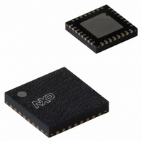
LPC1343FHN33,551 NXP Semiconductors, LPC1343FHN33,551 Datasheet - Page 233

LPC1343FHN33,551
Manufacturer Part Number
LPC1343FHN33,551
Description
IC MCU 32BIT 32KB FLASH 33HVQFN
Manufacturer
NXP Semiconductors
Series
LPC13xxr
Specifications of LPC1343FHN33,551
Program Memory Type
FLASH
Program Memory Size
32KB (32K x 8)
Package / Case
33-VQFN Exposed Pad, 33-HVQFN, 33-SQFN, 33-DHVQFN
Core Processor
ARM® Cortex-M3™
Core Size
32-Bit
Speed
72MHz
Connectivity
I²C, Microwire, SPI, SSI, SSP, UART/USART, USB
Peripherals
Brown-out Detect/Reset, POR, WDT
Number Of I /o
28
Ram Size
8K x 8
Voltage - Supply (vcc/vdd)
2 V ~ 3.6 V
Data Converters
A/D 8x10b
Oscillator Type
Internal
Operating Temperature
-40°C ~ 85°C
Processor Series
LPC13
Core
ARM Cortex M3
Data Bus Width
32 bit
Data Ram Size
8 KB
Interface Type
I2C, UART
Maximum Clock Frequency
72 MHz
Number Of Programmable I/os
28
Number Of Timers
4
Operating Supply Voltage
3.3 V
Maximum Operating Temperature
+ 85 C
Mounting Style
SMD/SMT
3rd Party Development Tools
MDK-ARM, RL-ARM, ULINK2, KSK-LPC1343
Development Tools By Supplier
OM11039, OM11040, OM11046, OM11048
Minimum Operating Temperature
- 40 C
On-chip Adc
10 bit, 8 Channel
Package
33HVQFN EP
Device Core
ARM Cortex M3
Family Name
LPC1000
Maximum Speed
72 MHz
Lead Free Status / RoHS Status
Lead free / RoHS Compliant
For Use With
622-1005 - USB IN-CIRCUIT PROG ARM7 LPC2K
Eeprom Size
-
Lead Free Status / Rohs Status
Lead free / RoHS Compliant
Other names
568-4944
935289655551
935289655551
Available stocks
Company
Part Number
Manufacturer
Quantity
Price
Company:
Part Number:
LPC1343FHN33,551
Manufacturer:
NXP
Quantity:
780
- Current page: 233 of 331
- Download datasheet (2Mb)
13.1 How to read this chapter
13.2 Basic configuration
13.3 Features
13.4 General description
UM10375
User manual
The SSP block is identical for all LPC13xx parts.
The SSP is configured using the following registers:
The SSP is a Synchronous Serial Port (SSP) controller capable of operation on a SPI,
4-wire SSI, or Microwire bus. It can interact with multiple masters and slaves on the bus.
Only a single master and a single slave can communicate on the bus during a given data
transfer. Data transfers are in principle full duplex, with frames of 4 bits to 16 bits of data
flowing from the master to the slave and from the slave to the master. In practice it is often
the case that only one of these data flows carries meaningful data.
The LPC13xx has one Synchronous Serial Port controller.
1. Pins: The SSP pins must be configured in the IOCONFIG register block
2. Power: In the SYSAHBCLKCTRL register, set bit 11
3. Peripheral clock: Enable the SSP peripheral clock by writing to the SSP0CLKDIV
4. Reset: Before accessing the SSP block, ensure that the SSP_RST_N bit (bit 0) in the
•
•
•
•
•
UM10375
Chapter 13: LPC13xx SSP
Rev. 2 — 7 July 2010
(Section
register
PRESETCTRL register
SSP block.
Compatible with Motorola SPI, 4-wire TI SSI, and National Semiconductor Microwire
buses.
Synchronous Serial Communication.
Supports master or slave operation.
Eight frame FIFOs for both transmit and receive.
4-bit to 16-bit frame.
(Table
6.4.1).
All information provided in this document is subject to legal disclaimers.
24).
Rev. 2 — 7 July 2010
(Table
7) is set to 1. This de-asserts the reset signal to the
(Table
23).
© NXP B.V. 2010. All rights reserved.
User manual
235 of 333
Related parts for LPC1343FHN33,551
Image
Part Number
Description
Manufacturer
Datasheet
Request
R

Part Number:
Description:
MCU, MPU & DSP Development Tools KICKSTART KIT NXP LPC1343
Manufacturer:
IAR Systems
Part Number:
Description:
NXP Semiconductors designed the LPC2420/2460 microcontroller around a 16-bit/32-bitARM7TDMI-S CPU core with real-time debug interfaces that include both JTAG andembedded trace
Manufacturer:
NXP Semiconductors
Datasheet:

Part Number:
Description:
NXP Semiconductors designed the LPC2458 microcontroller around a 16-bit/32-bitARM7TDMI-S CPU core with real-time debug interfaces that include both JTAG andembedded trace
Manufacturer:
NXP Semiconductors
Datasheet:
Part Number:
Description:
NXP Semiconductors designed the LPC2468 microcontroller around a 16-bit/32-bitARM7TDMI-S CPU core with real-time debug interfaces that include both JTAG andembedded trace
Manufacturer:
NXP Semiconductors
Datasheet:
Part Number:
Description:
NXP Semiconductors designed the LPC2470 microcontroller, powered by theARM7TDMI-S core, to be a highly integrated microcontroller for a wide range ofapplications that require advanced communications and high quality graphic displays
Manufacturer:
NXP Semiconductors
Datasheet:
Part Number:
Description:
NXP Semiconductors designed the LPC2478 microcontroller, powered by theARM7TDMI-S core, to be a highly integrated microcontroller for a wide range ofapplications that require advanced communications and high quality graphic displays
Manufacturer:
NXP Semiconductors
Datasheet:
Part Number:
Description:
The Philips Semiconductors XA (eXtended Architecture) family of 16-bit single-chip microcontrollers is powerful enough to easily handle the requirements of high performance embedded applications, yet inexpensive enough to compete in the market for hi
Manufacturer:
NXP Semiconductors
Datasheet:
Part Number:
Description:
The XA-S3 device is a member of Philips Semiconductors? XA(eXtended Architecture) family of high performance 16-bitsingle-chip microcontrollers
Manufacturer:
NXP Semiconductors
Datasheet:

Part Number:
Description:
The NXP BlueStreak LH75401/LH75411 family consists of two low-cost 16/32-bit System-on-Chip (SoC) devices
Manufacturer:
NXP Semiconductors
Datasheet:

Part Number:
Description:
The NXP LPC3130/3131 combine an 180 MHz ARM926EJ-S CPU core, high-speed USB2
Manufacturer:
NXP Semiconductors
Datasheet:

Part Number:
Description:
The NXP LPC3141 combine a 270 MHz ARM926EJ-S CPU core, High-speed USB 2
Manufacturer:
NXP Semiconductors

Part Number:
Description:
The NXP LPC3143 combine a 270 MHz ARM926EJ-S CPU core, High-speed USB 2
Manufacturer:
NXP Semiconductors

Part Number:
Description:
The NXP LPC3152 combines an 180 MHz ARM926EJ-S CPU core, High-speed USB 2
Manufacturer:
NXP Semiconductors

Part Number:
Description:
The NXP LPC3154 combines an 180 MHz ARM926EJ-S CPU core, High-speed USB 2
Manufacturer:
NXP Semiconductors


