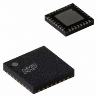
LPC1343FHN33,551 NXP Semiconductors, LPC1343FHN33,551 Datasheet - Page 287
LPC1343FHN33,551
Manufacturer Part Number
LPC1343FHN33,551
Description
IC MCU 32BIT 32KB FLASH 33HVQFN
Manufacturer
NXP Semiconductors
Series
LPC13xxr
Specifications of LPC1343FHN33,551
Program Memory Type
FLASH
Program Memory Size
32KB (32K x 8)
Package / Case
33-VQFN Exposed Pad, 33-HVQFN, 33-SQFN, 33-DHVQFN
Core Processor
ARM® Cortex-M3™
Core Size
32-Bit
Speed
72MHz
Connectivity
I²C, Microwire, SPI, SSI, SSP, UART/USART, USB
Peripherals
Brown-out Detect/Reset, POR, WDT
Number Of I /o
28
Ram Size
8K x 8
Voltage - Supply (vcc/vdd)
2 V ~ 3.6 V
Data Converters
A/D 8x10b
Oscillator Type
Internal
Operating Temperature
-40°C ~ 85°C
Processor Series
LPC13
Core
ARM Cortex M3
Data Bus Width
32 bit
Data Ram Size
8 KB
Interface Type
I2C, UART
Maximum Clock Frequency
72 MHz
Number Of Programmable I/os
28
Number Of Timers
4
Operating Supply Voltage
3.3 V
Maximum Operating Temperature
+ 85 C
Mounting Style
SMD/SMT
3rd Party Development Tools
MDK-ARM, RL-ARM, ULINK2, KSK-LPC1343
Development Tools By Supplier
OM11039, OM11040, OM11046, OM11048
Minimum Operating Temperature
- 40 C
On-chip Adc
10 bit, 8 Channel
Package
33HVQFN EP
Device Core
ARM Cortex M3
Family Name
LPC1000
Maximum Speed
72 MHz
Lead Free Status / RoHS Status
Lead free / RoHS Compliant
For Use With
622-1005 - USB IN-CIRCUIT PROG ARM7 LPC2K
Eeprom Size
-
Lead Free Status / Rohs Status
Lead free / RoHS Compliant
Other names
568-4944
935289655551
935289655551
Available stocks
Company
Part Number
Manufacturer
Quantity
Price
Company:

Part Number:
LPC1343FHN33,551
Manufacturer:
NXP
Quantity:
780


NXP Semiconductors
18.7 Operation
UM10375
User manual
18.7.1 Hardware-triggered conversion
18.7.2 Interrupts
Table 283: A/D Data Registers (AD0DR0 to AD0DR7 - addresses 0x4001 C010 to
If the BURST bit in the ADCR0 is 0 and the START field contains 010-111, the A/D
converter will start a conversion when a transition occurs on a selected pin or timer match
signal.
An interrupt is requested to the interrupt controller when the ADINT bit in the ADSTAT
register is 1. The ADINT bit is one when any of the DONE bits of A/D channels that are
enabled for interrupts (via the ADINTEN register) are one. Software can use the Interrupt
Enable bit in the interrupt controller that corresponds to the ADC to control whether this
results in an interrupt. The result register for an A/D channel that is generating an interrupt
must be read in order to clear the corresponding DONE flag.
Bit
5:0
15:6
29:16 -
30
31
Symbol
-
V_VREF
OVERRUN This bit is 1 in burst mode if the results of one or more conversions
DONE
0x4001 C02C) bit description
All information provided in this document is subject to legal disclaimers.
Description
Reserved.
When DONE is 1, this field contains a binary fraction representing the
voltage on the ADn pin, divided by the voltage on the V
the field indicates that the voltage on the ADn pin was less than, equal
to, or close to that on V
AD input was close to, equal to, or greater than that on V
Reserved.
was (were) lost and overwritten before the conversion that produced
the result in the V_VREF bits.This bit is cleared by reading this
register.
This bit is set to 1 when an A/D conversion completes. It is cleared
when this register is read.
Rev. 2 — 7 July 2010
Chapter 18: LPC13xx Analog-to-Digital Converter (ADC)
REF
, while 0x3FF indicates that the voltage on
REF
UM10375
REF
© NXP B.V. 2010. All rights reserved.
pin. Zero in
.
289 of 333
Reset
Value
0
NA
0
0
0
Related parts for LPC1343FHN33,551
Image
Part Number
Description
Manufacturer
Datasheet
Request
R

Part Number:
Description:
MCU, MPU & DSP Development Tools KICKSTART KIT NXP LPC1343
Manufacturer:
IAR Systems

Part Number:
Description:
NXP Semiconductors designed the LPC2420/2460 microcontroller around a 16-bit/32-bitARM7TDMI-S CPU core with real-time debug interfaces that include both JTAG andembedded trace
Manufacturer:
NXP Semiconductors
Datasheet:

Part Number:
Description:
NXP Semiconductors designed the LPC2458 microcontroller around a 16-bit/32-bitARM7TDMI-S CPU core with real-time debug interfaces that include both JTAG andembedded trace
Manufacturer:
NXP Semiconductors
Datasheet:
Part Number:
Description:
NXP Semiconductors designed the LPC2468 microcontroller around a 16-bit/32-bitARM7TDMI-S CPU core with real-time debug interfaces that include both JTAG andembedded trace
Manufacturer:
NXP Semiconductors
Datasheet:
Part Number:
Description:
NXP Semiconductors designed the LPC2470 microcontroller, powered by theARM7TDMI-S core, to be a highly integrated microcontroller for a wide range ofapplications that require advanced communications and high quality graphic displays
Manufacturer:
NXP Semiconductors
Datasheet:
Part Number:
Description:
NXP Semiconductors designed the LPC2478 microcontroller, powered by theARM7TDMI-S core, to be a highly integrated microcontroller for a wide range ofapplications that require advanced communications and high quality graphic displays
Manufacturer:
NXP Semiconductors
Datasheet:
Part Number:
Description:
The Philips Semiconductors XA (eXtended Architecture) family of 16-bit single-chip microcontrollers is powerful enough to easily handle the requirements of high performance embedded applications, yet inexpensive enough to compete in the market for hi
Manufacturer:
NXP Semiconductors
Datasheet:
Part Number:
Description:
The XA-S3 device is a member of Philips Semiconductors? XA(eXtended Architecture) family of high performance 16-bitsingle-chip microcontrollers
Manufacturer:
NXP Semiconductors
Datasheet:

Part Number:
Description:
The NXP BlueStreak LH75401/LH75411 family consists of two low-cost 16/32-bit System-on-Chip (SoC) devices
Manufacturer:
NXP Semiconductors
Datasheet:
Part Number:
Description:
The NXP LPC3130/3131 combine an 180 MHz ARM926EJ-S CPU core, high-speed USB2
Manufacturer:
NXP Semiconductors
Datasheet:
Part Number:
Description:
The NXP LPC3141 combine a 270 MHz ARM926EJ-S CPU core, High-speed USB 2
Manufacturer:
NXP Semiconductors
Part Number:
Description:
The NXP LPC3143 combine a 270 MHz ARM926EJ-S CPU core, High-speed USB 2
Manufacturer:
NXP Semiconductors

Part Number:
Description:
The NXP LPC3152 combines an 180 MHz ARM926EJ-S CPU core, High-speed USB 2
Manufacturer:
NXP Semiconductors
Part Number:
Description:
The NXP LPC3154 combines an 180 MHz ARM926EJ-S CPU core, High-speed USB 2
Manufacturer:
NXP Semiconductors