D12332VFC20V Renesas Electronics America, D12332VFC20V Datasheet - Page 1032
D12332VFC20V
Manufacturer Part Number
D12332VFC20V
Description
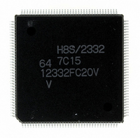
IC H8S/2332 MCU ROMLESS 144QFP
Manufacturer
Renesas Electronics America
Series
H8® H8S/2300r
Specifications of D12332VFC20V
Core Processor
H8S/2000
Core Size
16-Bit
Speed
20MHz
Connectivity
SCI, SmartCard
Peripherals
DMA, POR, PWM, WDT
Number Of I /o
106
Program Memory Type
ROMless
Ram Size
8K x 8
Voltage - Supply (vcc/vdd)
2.7 V ~ 3.6 V
Data Converters
A/D 12x10b; D/A 4x8b
Oscillator Type
Internal
Operating Temperature
-20°C ~ 75°C
Package / Case
144-QFP
For Use With
EDK2329 - DEV EVALUATION KIT H8S/2329
Lead Free Status / RoHS Status
Lead free / RoHS Compliant
Eeprom Size
-
Program Memory Size
-
Available stocks
Company
Part Number
Manufacturer
Quantity
Price
Company:

Part Number:
D12332VFC20V
Manufacturer:
Renesas Electronics America
Quantity:
10 000


Address
H'FFE8
H'FFE9
H'FFEA
H'FFEB
H'FFF0
H'FFF1
H'FFF2
H'FFF4
H'FFF5
H'FFF6
H'FFF7
H'FFF8
H'FFF9
H'FFFA
H'FFFB
Notes: 1. Located in on-chip RAM. The bus width is 32 bits when the DTC accesses this area as
Rev.4.00 Sep. 07, 2007 Page 1000 of 1210
REJ09B0245-0400
Register
Name
TGR1A
TGR1B
TCR2
TMDR2
TIOR2
TIER2
TSR2
TCNT2
TGR2A
TGR2B
2. Valid only in F-ZTAT version.
3. If the pulse output group 2 and pulse output group 3 output triggers are the same
4. Functions as C/A for SCI use, and as GM for smart card interface use.
5. Functions as CHR for SCI use, and as BLK for smart card interface use.
6. Functions as STOP for SCI use, and as BCP1 for smart card interface use.
7. Functions as MP for SCI use, and as BCP0 for smart card interface use.
8. Functions as FER for SCI use, and as ERS for smart card interface use.
9. Valid only in H8S/2339 F-ZTAT.
10. Valid only in H8S/2338 F-ZTAT.
register information, and 16 bits otherwise.
according to the PCR setting, the NDRH address will be H'FF4C, and if different, the
address of NDRH for group 2 will be H'FF4E, and that for group 3 will be H'FF4C.
Similarly, if the pulse output group 0 and pulse output group 1 output triggers are the
same according to the PCR setting, the NDRL address will be H'FF4D, and if different,
the address of NDRL for group 0 will be H'FF4F, and that for group 1 will be H'FF4D.
Bit 7
—
—
IOB3
TTGE
TCFD
Bit 6
CCLR1
—
IOB2
—
—
Bit 5
CCLR0
—
IOB1
TCIEU
TCFU
Bit 4
CKEG1
—
IOB0
TCIEV
TCFV
Bit 3
CKEG0
MD3
IOA3
—
—
Bit 2
TPSC2
MD2
IOA2
—
—
Bit 1
TPSC1
MD1
IOA1
TGIEB
TGFB
Bit 0
TPSC0
MD0
IOA0
TGIEA
TGFA
Module
Name
TPU1
TPU2
Data
Bus
Width
16 bits
16 bits
Related parts for D12332VFC20V
Image
Part Number
Description
Manufacturer
Datasheet
Request
R

Part Number:
Description:
KIT STARTER FOR M16C/29
Manufacturer:
Renesas Electronics America
Datasheet:

Part Number:
Description:
KIT STARTER FOR R8C/2D
Manufacturer:
Renesas Electronics America
Datasheet:

Part Number:
Description:
R0K33062P STARTER KIT
Manufacturer:
Renesas Electronics America
Datasheet:

Part Number:
Description:
KIT STARTER FOR R8C/23 E8A
Manufacturer:
Renesas Electronics America
Datasheet:

Part Number:
Description:
KIT STARTER FOR R8C/25
Manufacturer:
Renesas Electronics America
Datasheet:

Part Number:
Description:
KIT STARTER H8S2456 SHARPE DSPLY
Manufacturer:
Renesas Electronics America
Datasheet:

Part Number:
Description:
KIT STARTER FOR R8C38C
Manufacturer:
Renesas Electronics America
Datasheet:

Part Number:
Description:
KIT STARTER FOR R8C35C
Manufacturer:
Renesas Electronics America
Datasheet:

Part Number:
Description:
KIT STARTER FOR R8CL3AC+LCD APPS
Manufacturer:
Renesas Electronics America
Datasheet:
Part Number:
Description:
KIT STARTER FOR RX610
Manufacturer:
Renesas Electronics America
Datasheet:

Part Number:
Description:
KIT STARTER FOR R32C/118
Manufacturer:
Renesas Electronics America
Datasheet:

Part Number:
Description:
KIT DEV RSK-R8C/26-29
Manufacturer:
Renesas Electronics America
Datasheet:

Part Number:
Description:
KIT STARTER FOR SH7124
Manufacturer:
Renesas Electronics America
Datasheet:

Part Number:
Description:
KIT STARTER FOR H8SX/1622
Manufacturer:
Renesas Electronics America
Datasheet:

Part Number:
Description:
KIT DEV FOR SH7203
Manufacturer:
Renesas Electronics America
Datasheet: