D12332VFC20V Renesas Electronics America, D12332VFC20V Datasheet - Page 17
D12332VFC20V
Manufacturer Part Number
D12332VFC20V
Description
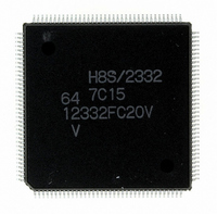
IC H8S/2332 MCU ROMLESS 144QFP
Manufacturer
Renesas Electronics America
Series
H8® H8S/2300r
Specifications of D12332VFC20V
Core Processor
H8S/2000
Core Size
16-Bit
Speed
20MHz
Connectivity
SCI, SmartCard
Peripherals
DMA, POR, PWM, WDT
Number Of I /o
106
Program Memory Type
ROMless
Ram Size
8K x 8
Voltage - Supply (vcc/vdd)
2.7 V ~ 3.6 V
Data Converters
A/D 12x10b; D/A 4x8b
Oscillator Type
Internal
Operating Temperature
-20°C ~ 75°C
Package / Case
144-QFP
For Use With
EDK2329 - DEV EVALUATION KIT H8S/2329
Lead Free Status / RoHS Status
Lead free / RoHS Compliant
Eeprom Size
-
Program Memory Size
-
Available stocks
Company
Part Number
Manufacturer
Quantity
Price
Company:

Part Number:
D12332VFC20V
Manufacturer:
Renesas Electronics America
Quantity:
10 000


6.6
6.7
6.8
6.9
6.10 Bus Release....................................................................................................................... 194
6.11 Bus Arbitration.................................................................................................................. 197
6.12 Resets and Bus Controller................................................................................................. 199
Section 7 DMA Controller
7.1
7.2
6.5.7
6.5.8
6.5.9
6.5.10 Burst Operation.................................................................................................... 176
6.5.11 Refresh Control.................................................................................................... 179
DMAC Single Address Mode and DRAM Interface ........................................................ 183
6.6.1
6.6.2
Burst ROM Interface......................................................................................................... 185
6.7.1
6.7.2
6.7.3
Idle Cycle .......................................................................................................................... 188
6.8.1
6.8.2
Write Data Buffer Function .............................................................................................. 193
6.10.1 Overview.............................................................................................................. 194
6.10.2 Operation ............................................................................................................. 194
6.10.3 Pin States in External-Bus-Released State ........................................................... 195
6.10.4 Transition Timing ................................................................................................ 196
6.10.5 Usage Note........................................................................................................... 197
6.11.1 Overview.............................................................................................................. 197
6.11.2 Operation ............................................................................................................. 197
6.11.3 Bus Transfer Timing ............................................................................................ 198
6.11.4 External Bus Release Usage Note........................................................................ 198
Overview........................................................................................................................... 201
7.1.1
7.1.2
7.1.3
7.1.4
7.1.5
Register Descriptions (1) (Short Address Mode) .............................................................. 207
7.2.1
7.2.2
7.2.3
Precharge State Control ....................................................................................... 171
Wait Control ........................................................................................................ 172
Byte Access Control ............................................................................................ 174
When DDS = 1..................................................................................................... 183
When DDS = 0..................................................................................................... 184
Overview.............................................................................................................. 185
Basic Timing........................................................................................................ 185
Wait Control ........................................................................................................ 187
Operation ............................................................................................................. 188
Pin States in Idle Cycle ........................................................................................ 192
Features................................................................................................................ 201
Block Diagram..................................................................................................... 202
Overview of Functions......................................................................................... 203
Pin Configuration................................................................................................. 205
Register Configuration......................................................................................... 206
Memory Address Registers (MAR) ..................................................................... 208
I/O Address Register (IOAR) .............................................................................. 209
Execute Transfer Count Register (ETCR) ........................................................... 209
................................................................................................ 201
Rev.4.00 Sep. 07, 2007 Page xv of xxx
Related parts for D12332VFC20V
Image
Part Number
Description
Manufacturer
Datasheet
Request
R

Part Number:
Description:
KIT STARTER FOR M16C/29
Manufacturer:
Renesas Electronics America
Datasheet:

Part Number:
Description:
KIT STARTER FOR R8C/2D
Manufacturer:
Renesas Electronics America
Datasheet:

Part Number:
Description:
R0K33062P STARTER KIT
Manufacturer:
Renesas Electronics America
Datasheet:

Part Number:
Description:
KIT STARTER FOR R8C/23 E8A
Manufacturer:
Renesas Electronics America
Datasheet:

Part Number:
Description:
KIT STARTER FOR R8C/25
Manufacturer:
Renesas Electronics America
Datasheet:

Part Number:
Description:
KIT STARTER H8S2456 SHARPE DSPLY
Manufacturer:
Renesas Electronics America
Datasheet:

Part Number:
Description:
KIT STARTER FOR R8C38C
Manufacturer:
Renesas Electronics America
Datasheet:

Part Number:
Description:
KIT STARTER FOR R8C35C
Manufacturer:
Renesas Electronics America
Datasheet:

Part Number:
Description:
KIT STARTER FOR R8CL3AC+LCD APPS
Manufacturer:
Renesas Electronics America
Datasheet:
Part Number:
Description:
KIT STARTER FOR RX610
Manufacturer:
Renesas Electronics America
Datasheet:

Part Number:
Description:
KIT STARTER FOR R32C/118
Manufacturer:
Renesas Electronics America
Datasheet:

Part Number:
Description:
KIT DEV RSK-R8C/26-29
Manufacturer:
Renesas Electronics America
Datasheet:

Part Number:
Description:
KIT STARTER FOR SH7124
Manufacturer:
Renesas Electronics America
Datasheet:

Part Number:
Description:
KIT STARTER FOR H8SX/1622
Manufacturer:
Renesas Electronics America
Datasheet:

Part Number:
Description:
KIT DEV FOR SH7203
Manufacturer:
Renesas Electronics America
Datasheet: