D12332VFC20V Renesas Electronics America, D12332VFC20V Datasheet - Page 573
D12332VFC20V
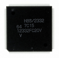
Manufacturer Part Number
D12332VFC20V
Description
IC H8S/2332 MCU ROMLESS 144QFP
Manufacturer
Renesas Electronics America
Series
H8® H8S/2300r
Specifications of D12332VFC20V
Core Processor
H8S/2000
Core Size
16-Bit
Speed
20MHz
Connectivity
SCI, SmartCard
Peripherals
DMA, POR, PWM, WDT
Number Of I /o
106
Program Memory Type
ROMless
Ram Size
8K x 8
Voltage - Supply (vcc/vdd)
2.7 V ~ 3.6 V
Data Converters
A/D 12x10b; D/A 4x8b
Oscillator Type
Internal
Operating Temperature
-20°C ~ 75°C
Package / Case
144-QFP
For Use With
EDK2329 - DEV EVALUATION KIT H8S/2329
Lead Free Status / RoHS Status
Lead free / RoHS Compliant
Eeprom Size
-
Program Memory Size
-
Available stocks
Company
Part Number
Manufacturer
Quantity
Price
Company:

Part Number:
D12332VFC20V
Manufacturer:
Renesas Electronics America
Quantity:
10 000


Bit 1—Group 1 Non-Overlap (G1NOV): Selects normal or non-overlapping operation for pulse
output group 1 (pins PO7 to PO4).
Bit 1
G1NOV
0
1
Bit 0—Group 0 Non-Overlap (G0NOV): Selects normal or non-overlapping operation for pulse
output group 0 (pins PO3 to PO0).
Bit 0
G0NOV
0
1
11.2.7
P1DDR is an 8-bit write-only register, the individual bits of which specify input or output for the
pins of port 1.
Port 1 is multiplexed with pins PO15 to PO8. Bits corresponding to pins used for PPG output must
be set to 1. For further information about P1DDR, see section 9, I/O Port.
Bit
Initial value :
R/W
Port 1 Data Direction Register (P1DDR)
Description
in the selected TPU channel)
compare match A or B in the selected TPU channel)
Description
in the selected TPU channel)
compare match A or B in the selected TPU channel)
Normal operation in pulse output group 1 (output values updated at compare match A
Non-overlapping operation in pulse output group 1 (independent 1 and 0 output at
Normal operation in pulse output group 0 (output values updated at compare match A
Non-overlapping operation in pulse output group 0 (independent 1 and 0 output at
:
:
P17DDR P16DDR P15DDR P14DDR P13DDR P12DDR P11DDR P10DDR
W
7
0
W
6
0
W
5
0
W
0
4
Rev.4.00 Sep. 07, 2007 Page 541 of 1210
W
3
0
W
2
0
REJ09B0245-0400
W
1
0
(Initial value)
(Initial value)
W
0
0
Related parts for D12332VFC20V
Image
Part Number
Description
Manufacturer
Datasheet
Request
R

Part Number:
Description:
KIT STARTER FOR M16C/29
Manufacturer:
Renesas Electronics America
Datasheet:

Part Number:
Description:
KIT STARTER FOR R8C/2D
Manufacturer:
Renesas Electronics America
Datasheet:

Part Number:
Description:
R0K33062P STARTER KIT
Manufacturer:
Renesas Electronics America
Datasheet:

Part Number:
Description:
KIT STARTER FOR R8C/23 E8A
Manufacturer:
Renesas Electronics America
Datasheet:

Part Number:
Description:
KIT STARTER FOR R8C/25
Manufacturer:
Renesas Electronics America
Datasheet:

Part Number:
Description:
KIT STARTER H8S2456 SHARPE DSPLY
Manufacturer:
Renesas Electronics America
Datasheet:

Part Number:
Description:
KIT STARTER FOR R8C38C
Manufacturer:
Renesas Electronics America
Datasheet:

Part Number:
Description:
KIT STARTER FOR R8C35C
Manufacturer:
Renesas Electronics America
Datasheet:

Part Number:
Description:
KIT STARTER FOR R8CL3AC+LCD APPS
Manufacturer:
Renesas Electronics America
Datasheet:
Part Number:
Description:
KIT STARTER FOR RX610
Manufacturer:
Renesas Electronics America
Datasheet:

Part Number:
Description:
KIT STARTER FOR R32C/118
Manufacturer:
Renesas Electronics America
Datasheet:

Part Number:
Description:
KIT DEV RSK-R8C/26-29
Manufacturer:
Renesas Electronics America
Datasheet:

Part Number:
Description:
KIT STARTER FOR SH7124
Manufacturer:
Renesas Electronics America
Datasheet:

Part Number:
Description:
KIT STARTER FOR H8SX/1622
Manufacturer:
Renesas Electronics America
Datasheet:

Part Number:
Description:
KIT DEV FOR SH7203
Manufacturer:
Renesas Electronics America
Datasheet: