D12332VFC20V Renesas Electronics America, D12332VFC20V Datasheet - Page 735
D12332VFC20V
Manufacturer Part Number
D12332VFC20V
Description
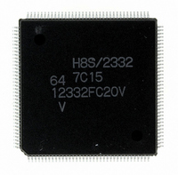
IC H8S/2332 MCU ROMLESS 144QFP
Manufacturer
Renesas Electronics America
Series
H8® H8S/2300r
Specifications of D12332VFC20V
Core Processor
H8S/2000
Core Size
16-Bit
Speed
20MHz
Connectivity
SCI, SmartCard
Peripherals
DMA, POR, PWM, WDT
Number Of I /o
106
Program Memory Type
ROMless
Ram Size
8K x 8
Voltage - Supply (vcc/vdd)
2.7 V ~ 3.6 V
Data Converters
A/D 12x10b; D/A 4x8b
Oscillator Type
Internal
Operating Temperature
-20°C ~ 75°C
Package / Case
144-QFP
For Use With
EDK2329 - DEV EVALUATION KIT H8S/2329
Lead Free Status / RoHS Status
Lead free / RoHS Compliant
Eeprom Size
-
Program Memory Size
-
Available stocks
Company
Part Number
Manufacturer
Quantity
Price
Company:

Part Number:
D12332VFC20V
Manufacturer:
Renesas Electronics America
Quantity:
10 000


16.2
16.2.1
There are four 16-bit read-only ADDR registers, ADDRA to ADDRD, used to store the results of
A/D conversion.
The 10-bit data resulting from A/D conversion is transferred to the ADDR register for the selected
channel and stored there. The upper 8 bits of the converted data are transferred to the upper byte
(bits 15 to 8) of ADDR, and the lower 2 bits are transferred to the lower byte (bits 7 and 6) and
stored. Bits 5 to 0 are always read as 0.
The correspondence between the analog input channels and ADDR registers is shown in table
16.3.
The ADDR registers can always be read by the CPU. The upper byte can be read directly, but for
the lower byte, data transfer is performed via a temporary register (TEMP). For details, see section
16.3, Interface to Bus Master.
The ADDR registers are initialized to H'0000 by a reset, and in standby mode or module stop
mode.
Table 16.3 Analog Input Channels and Corresponding ADDR Registers
Group 0
(CH2 = 0)
AN0
AN1
AN2
AN3
Bit
Initial value :
R/W
Channel Set 0 (CH3 = 1)
Register Descriptions
A/D Data Registers A to D (ADDRA to ADDRD)
:
:
AD9 AD8 AD7 AD6 AD5 AD4 AD3 AD2 AD1 AD0 —
Group 1
(CH2 = 1)
AN4
AN5
AN6
AN7
15
R
0
14
R
0
Analog Input Channel
13
R
0
12
R
0
Group 0
(CH2 = 0)
Setting prohibited
Setting prohibited
Setting prohibited
Setting prohibited
11
R
0
10
R
0
Channel Set 1 (CH3 = 0)
R
9
0
R
8
0
Rev.4.00 Sep. 07, 2007 Page 703 of 1210
Group 1
(CH2 = 1)
AN12
AN13
AN14
AN15
R
7
0
R
6
0
R
5
0
—
R
4
0
A/D Data Register
ADDRA
ADDRB
ADDRC
ADDRD
—
REJ09B0245-0400
R
3
0
—
R
2
0
—
R
1
0
—
R
0
0
Related parts for D12332VFC20V
Image
Part Number
Description
Manufacturer
Datasheet
Request
R

Part Number:
Description:
KIT STARTER FOR M16C/29
Manufacturer:
Renesas Electronics America
Datasheet:

Part Number:
Description:
KIT STARTER FOR R8C/2D
Manufacturer:
Renesas Electronics America
Datasheet:

Part Number:
Description:
R0K33062P STARTER KIT
Manufacturer:
Renesas Electronics America
Datasheet:

Part Number:
Description:
KIT STARTER FOR R8C/23 E8A
Manufacturer:
Renesas Electronics America
Datasheet:

Part Number:
Description:
KIT STARTER FOR R8C/25
Manufacturer:
Renesas Electronics America
Datasheet:

Part Number:
Description:
KIT STARTER H8S2456 SHARPE DSPLY
Manufacturer:
Renesas Electronics America
Datasheet:

Part Number:
Description:
KIT STARTER FOR R8C38C
Manufacturer:
Renesas Electronics America
Datasheet:

Part Number:
Description:
KIT STARTER FOR R8C35C
Manufacturer:
Renesas Electronics America
Datasheet:

Part Number:
Description:
KIT STARTER FOR R8CL3AC+LCD APPS
Manufacturer:
Renesas Electronics America
Datasheet:
Part Number:
Description:
KIT STARTER FOR RX610
Manufacturer:
Renesas Electronics America
Datasheet:

Part Number:
Description:
KIT STARTER FOR R32C/118
Manufacturer:
Renesas Electronics America
Datasheet:

Part Number:
Description:
KIT DEV RSK-R8C/26-29
Manufacturer:
Renesas Electronics America
Datasheet:

Part Number:
Description:
KIT STARTER FOR SH7124
Manufacturer:
Renesas Electronics America
Datasheet:

Part Number:
Description:
KIT STARTER FOR H8SX/1622
Manufacturer:
Renesas Electronics America
Datasheet:

Part Number:
Description:
KIT DEV FOR SH7203
Manufacturer:
Renesas Electronics America
Datasheet: