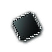
PIC18F87J72-I/PT Microchip Technology, PIC18F87J72-I/PT Datasheet - Page 13

PIC18F87J72-I/PT
Manufacturer Part Number
PIC18F87J72-I/PT
Description
IC PIC MCU 8BIT 14KB FLSH 80TQFP
Manufacturer
Microchip Technology
Series
PIC® 18Fr
Datasheet
1.PIC18F86J72-IPT.pdf
(480 pages)
Specifications of PIC18F87J72-I/PT
Program Memory Type
FLASH
Program Memory Size
128KB (64K x 16)
Package / Case
80-TQFP
Core Processor
PIC
Core Size
8-Bit
Speed
48MHz
Connectivity
I²C, LIN, SPI, UART/USART
Peripherals
Brown-out Detect/Reset, LCD, LVD, POR, PWM, WDT
Number Of I /o
51
Ram Size
3.8K x 8
Voltage - Supply (vcc/vdd)
2 V ~ 3.6 V
Data Converters
A/D 12x12b
Oscillator Type
Internal
Operating Temperature
-40°C ~ 85°C
Data Bus Width
8 bit
Data Ram Size
4 KB
Interface Type
SPI, USART, SPI, I2C
Maximum Clock Frequency
8 MHz
Number Of Programmable I/os
51
Number Of Timers
4
Operating Supply Voltage
2 V to 3.6 V
Maximum Operating Temperature
+ 85 C
Mounting Style
SMD/SMT
Minimum Operating Temperature
- 40 C
On-chip Adc
14
Controller Family/series
PIC18F
No. Of I/o's
51
Ram Memory Size
3923Byte
Cpu Speed
48MHz
No. Of Timers
4
Rohs Compliant
Yes
Lead Free Status / RoHS Status
Lead free / RoHS Compliant
Lead Free Status / RoHS Status
Lead free / RoHS Compliant, Lead free / RoHS Compliant
Available stocks
Company
Part Number
Manufacturer
Quantity
Price
Company:
Part Number:
PIC18F87J72-I/PT
Manufacturer:
Microchip
Quantity:
210
Company:
Part Number:
PIC18F87J72-I/PT
Manufacturer:
Microchip Technology
Quantity:
10 000
- Current page: 13 of 480
- Download datasheet (5Mb)
TABLE 1-2:
2010 Microchip Technology Inc.
MCLR
OSC1/CLKI/RA7
OSC2/CLKO/RA6
RA0/AN0
RA1/AN1/SEG18
RA2/AN2/V
RA3/AN3/V
RA4/T0CKI/SEG14
RA5/AN4/SEG15
RA6
RA7
Legend: TTL = TTL compatible input
Note 1:
OSC1
CLKI
RA7
OSC2
CLKO
RA6
RA0
AN0
RA1
AN1
SEG18
RA2
AN2
V
RA3
AN3
V
RA4
T0CKI
SEG14
RA5
AN4
SEG15
REF
REF
Pin Name
2:
-
+
ST
I2C
I
P
Default assignment for CCP2 when the CCP2MX Configuration bit is set.
Alternate assignment for CCP2 when the CCP2MX Configuration bit is cleared.
REF
REF
-
+
= Schmitt Trigger input with CMOS levels
= I
= Input
= Power
PIC18F8XJ72 PINOUT I/O DESCRIPTIONS
2
C/SMBus compatible input
Pin Number
TQFP
48
49
31
30
27
25
34
33
9
Type
Pin
I/O
I/O
I/O
I/O
I/O
I/O
I/O
I/O
O
O
O
O
O
I
I
I
I
I
I
I
I
I
I
I
Analog
Analog
Analog
Analog
Analog
Analog
Analog
Analog
Analog
Analog
Buffer
CMOS
CMOS
Type
TTL
TTL
TTL
TTL
TTL
TTL
TTL
ST
ST
ST
—
—
Preliminary
Master Clear (input) or programming voltage (input). This pin
is an active-low Reset to the device.
Oscillator crystal or external clock input.
Oscillator crystal or clock output.
PORTA is a bidirectional I/O port.
Oscillator crystal input.
External clock source input. Always associated
with pin function, OSC1. (See related OSC1/CLKI,
OSC2/CLKO pins.)
General purpose I/O pin.
Oscillator crystal output. Connects to crystal or
resonator in Crystal Oscillator mode.
In EC modes, OSC2 pin outputs CLKO, which has
1/4 the frequency of OSC1 and denotes the
instruction cycle rate.
General purpose I/O pin.
Digital I/O.
Analog Input 0.
Digital I/O.
Analog Input 1.
SEG18 output for LCD.
Digital I/O.
Analog Input 2.
A/D reference voltage (low) input.
Digital I/O.
Analog Input 3.
A/D reference voltage (high) input.
Digital I/O.
Timer0 external clock input.
SEG14 output for LCD.
Digital I/O.
Analog Input 4.
SEG15 output for LCD.
See the OSC2/CLKO/RA6 pin.
See the OSC1/CLKI/RA7 pin.
PIC18F87J72 FAMILY
OD
CMOS = CMOS compatible input or output
Analog = Analog input
O
= Open-Drain (no P diode to V
= Output
Description
DS39979A-page 13
DD
)
Related parts for PIC18F87J72-I/PT
Image
Part Number
Description
Manufacturer
Datasheet
Request
R

Part Number:
Description:
Manufacturer:
Microchip Technology Inc.
Datasheet:

Part Number:
Description:
Manufacturer:
Microchip Technology Inc.
Datasheet:

Part Number:
Description:
Manufacturer:
Microchip Technology Inc.
Datasheet:

Part Number:
Description:
Manufacturer:
Microchip Technology Inc.
Datasheet:

Part Number:
Description:
Manufacturer:
Microchip Technology Inc.
Datasheet:

Part Number:
Description:
Manufacturer:
Microchip Technology Inc.
Datasheet:

Part Number:
Description:
Manufacturer:
Microchip Technology Inc.
Datasheet:

Part Number:
Description:
Manufacturer:
Microchip Technology Inc.
Datasheet:


