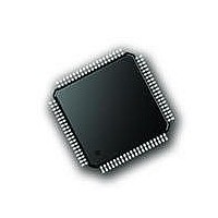
PIC18F87J72-I/PT Microchip Technology, PIC18F87J72-I/PT Datasheet - Page 461

PIC18F87J72-I/PT
Manufacturer Part Number
PIC18F87J72-I/PT
Description
IC PIC MCU 8BIT 14KB FLSH 80TQFP
Manufacturer
Microchip Technology
Series
PIC® 18Fr
Datasheet
1.PIC18F86J72-IPT.pdf
(480 pages)
Specifications of PIC18F87J72-I/PT
Program Memory Type
FLASH
Program Memory Size
128KB (64K x 16)
Package / Case
80-TQFP
Core Processor
PIC
Core Size
8-Bit
Speed
48MHz
Connectivity
I²C, LIN, SPI, UART/USART
Peripherals
Brown-out Detect/Reset, LCD, LVD, POR, PWM, WDT
Number Of I /o
51
Ram Size
3.8K x 8
Voltage - Supply (vcc/vdd)
2 V ~ 3.6 V
Data Converters
A/D 12x12b
Oscillator Type
Internal
Operating Temperature
-40°C ~ 85°C
Data Bus Width
8 bit
Data Ram Size
4 KB
Interface Type
SPI, USART, SPI, I2C
Maximum Clock Frequency
8 MHz
Number Of Programmable I/os
51
Number Of Timers
4
Operating Supply Voltage
2 V to 3.6 V
Maximum Operating Temperature
+ 85 C
Mounting Style
SMD/SMT
Minimum Operating Temperature
- 40 C
On-chip Adc
14
Controller Family/series
PIC18F
No. Of I/o's
51
Ram Memory Size
3923Byte
Cpu Speed
48MHz
No. Of Timers
4
Rohs Compliant
Yes
Lead Free Status / RoHS Status
Lead free / RoHS Compliant
Lead Free Status / RoHS Status
Lead free / RoHS Compliant, Lead free / RoHS Compliant
Available stocks
Company
Part Number
Manufacturer
Quantity
Price
Company:
Part Number:
PIC18F87J72-I/PT
Manufacturer:
Microchip
Quantity:
210
Company:
Part Number:
PIC18F87J72-I/PT
Manufacturer:
Microchip Technology
Quantity:
10 000
- Current page: 461 of 480
- Download datasheet (5Mb)
REGISTER B-4:
2010 Microchip Technology Inc.
bit 7
Legend:
R = Readable bit
-n = Value at POR
bit 7-6
bit 5
bit 4
bit 3-2
bit 1-0
READ<1>
R/W-1
READ: Address Loop Setting bits
11= Address counter loops on entire register map
10= Address counter loops on register TYPES (default)
01= Address counter loops on register GROUPS
00= Address not incremented, continually read same single register
DR_LTY: Data Ready Latency Control bit
1 = “No Latency” conversion, DR pulses after 3 DRCLK periods (default)
0 = Unsettled data is available after every DRCLK period
DR_HIZn: Data Ready Pin Inactive State Control bit
1 = The Data Ready pin default state is a logic high when data is NOT ready
0 = The Data Ready pin default state is high impedance when data is NOT ready (default)
DRMODE<1:0>: Data Ready Pin (DR) Control bits
11= Both data ready pulses from ADC0 and ADC Channel 1 are output on the DR pin
10= Data ready pulses from ADC Channel 1 are output on the DR pin; DR from ADC Channel 0 are
01= Data ready pulses from ADC Channel 0 are output on the DR pin; DR from ADC Channel 1 are
00= Data ready pulses from the lagging ADC between the two are output on the DR pin; the lagging
DRSTATUS<1:0>: Data Ready Status bits
11= ADC Channel 1 and Channel 0 data not ready (default)
10= ADC Channel 1 data not ready, ADC Channel 0 data ready
01= ADC Channel 0 data not ready, ADC Channel 1 data ready
00= ADC Channel 1 and Channel 0 data ready
READ<0>
R/W-0
not present on the pin
not present on the pin
ADC selection depends on the PHASE register and on the OSR (default)
STATUS AND COMMUNICATION REGISTER (ADDRESS 0x09)
W = Writable bit
‘1’ = Bit is set
DR_LTY
R/W-1
DR_HIZN
R/W-0
Preliminary
U = Unimplemented bit, read as ‘0’
‘0’ = Bit is cleared
DRMODE<1> DRMODE<0>
PIC18F87J72 FAMILY
R/W-0
R/W-0
x = Bit is unknown
DRSTATUS
R-1
<1>
DS39979A-page 461
DRSTATUS
R-1
<0>
bit 0
Related parts for PIC18F87J72-I/PT
Image
Part Number
Description
Manufacturer
Datasheet
Request
R

Part Number:
Description:
Manufacturer:
Microchip Technology Inc.
Datasheet:

Part Number:
Description:
Manufacturer:
Microchip Technology Inc.
Datasheet:

Part Number:
Description:
Manufacturer:
Microchip Technology Inc.
Datasheet:

Part Number:
Description:
Manufacturer:
Microchip Technology Inc.
Datasheet:

Part Number:
Description:
Manufacturer:
Microchip Technology Inc.
Datasheet:

Part Number:
Description:
Manufacturer:
Microchip Technology Inc.
Datasheet:

Part Number:
Description:
Manufacturer:
Microchip Technology Inc.
Datasheet:

Part Number:
Description:
Manufacturer:
Microchip Technology Inc.
Datasheet:


