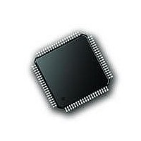
PIC18F87J72-I/PT Microchip Technology, PIC18F87J72-I/PT Datasheet - Page 295

PIC18F87J72-I/PT
Manufacturer Part Number
PIC18F87J72-I/PT
Description
IC PIC MCU 8BIT 14KB FLSH 80TQFP
Manufacturer
Microchip Technology
Series
PIC® 18Fr
Datasheet
1.PIC18F86J72-IPT.pdf
(480 pages)
Specifications of PIC18F87J72-I/PT
Program Memory Type
FLASH
Program Memory Size
128KB (64K x 16)
Package / Case
80-TQFP
Core Processor
PIC
Core Size
8-Bit
Speed
48MHz
Connectivity
I²C, LIN, SPI, UART/USART
Peripherals
Brown-out Detect/Reset, LCD, LVD, POR, PWM, WDT
Number Of I /o
51
Ram Size
3.8K x 8
Voltage - Supply (vcc/vdd)
2 V ~ 3.6 V
Data Converters
A/D 12x12b
Oscillator Type
Internal
Operating Temperature
-40°C ~ 85°C
Data Bus Width
8 bit
Data Ram Size
4 KB
Interface Type
SPI, USART, SPI, I2C
Maximum Clock Frequency
8 MHz
Number Of Programmable I/os
51
Number Of Timers
4
Operating Supply Voltage
2 V to 3.6 V
Maximum Operating Temperature
+ 85 C
Mounting Style
SMD/SMT
Minimum Operating Temperature
- 40 C
On-chip Adc
14
Controller Family/series
PIC18F
No. Of I/o's
51
Ram Memory Size
3923Byte
Cpu Speed
48MHz
No. Of Timers
4
Rohs Compliant
Yes
Lead Free Status / RoHS Status
Lead free / RoHS Compliant
Lead Free Status / RoHS Status
Lead free / RoHS Compliant, Lead free / RoHS Compliant
Available stocks
Company
Part Number
Manufacturer
Quantity
Price
Company:
Part Number:
PIC18F87J72-I/PT
Manufacturer:
Microchip
Quantity:
210
Company:
Part Number:
PIC18F87J72-I/PT
Manufacturer:
Microchip Technology
Quantity:
10 000
- Current page: 295 of 480
- Download datasheet (5Mb)
23.2
A single comparator is shown in Figure 23-2, along with
the relationship between the analog input levels and
the digital output. When the analog input at V
than the analog input V
is a digital low level. When the analog input at V
greater than the analog input V
comparator is a digital high level. The shaded areas of
the output of the comparator in Figure 23-2 represent
the uncertainty due to input offsets and response time.
23.3
Depending on the comparator operating mode, either
an external or internal voltage reference may be used.
The analog signal present at V
signal at V
is adjusted accordingly (Figure 23-2).
FIGURE 23-2:
23.3.1
When external voltage references are used, the
comparator module can be configured to have the com-
parators operate from the same or different reference
sources. However, threshold detector applications may
require the same reference. The reference signal must
be between V
pin of the comparator(s).
2010 Microchip Technology Inc.
V
V
Output
IN
IN
-
+
V
V
IN
IN
Comparator Operation
Comparator Reference
+
-
IN
EXTERNAL REFERENCE SIGNAL
+ and the digital output of the comparator
SS
and V
+
–
IN
SINGLE COMPARATOR
DD
-, the output of the comparator
and can be applied to either
IN
IN
- is compared to the
-, the output of the
Output
IN
+ is less
IN
+ is
Preliminary
PIC18F87J72 FAMILY
23.3.2
The comparator module also allows the selection of an
internally generated voltage reference from the
comparator voltage reference module. This module is
described in more detail in Section 24.0 “Comparator
Voltage Reference Module”.
The internal reference is only available in the mode
where four inputs are multiplexed to two comparators
(CM<2:0> = 110). In this mode, the internal voltage
reference is applied to the V
23.4
Response time is the minimum time, after selecting a
new reference voltage or input source, before the
comparator output has a valid level. If the internal ref-
erence is changed, the maximum delay of the internal
voltage reference must be considered when using the
comparator outputs. Otherwise, the maximum delay of
the comparators should be used (see Section 29.0
“Electrical Characteristics”).
23.5
The comparator outputs are read through the CMCON
register. These bits are read-only. The comparator
outputs may also be directly output to the RF1 and RF2
I/O pins. When enabled, multiplexers in the output path
of the RF1 and RF2 pins will switch and the output of
each pin will be the unsynchronized output of the
comparator.
comparators is related to the input offset voltage and
the response time given in the specifications.
Figure 23-3 shows the comparator output block
diagram.
The TRISF bits will still function as an output enable/
disable for the RF1 and RF2 pins while in this mode.
The polarity of the comparator outputs can be changed
using the C2INV and C1INV bits (CMCON<5:4>).
Note 1: When reading the PORT register, all pins
2: Analog levels on any pin defined as a
Comparator Response Time
Comparator Outputs
INTERNAL REFERENCE SIGNAL
configured as analog inputs will read as
‘0’. Pins configured as digital inputs will
convert an analog input according to the
Schmitt Trigger input specification.
digital input may cause the input buffer to
consume more current than is specified.
The
uncertainty
IN
+ pin of both comparators.
of
DS39979A-page 295
each
of
the
Related parts for PIC18F87J72-I/PT
Image
Part Number
Description
Manufacturer
Datasheet
Request
R

Part Number:
Description:
Manufacturer:
Microchip Technology Inc.
Datasheet:

Part Number:
Description:
Manufacturer:
Microchip Technology Inc.
Datasheet:

Part Number:
Description:
Manufacturer:
Microchip Technology Inc.
Datasheet:

Part Number:
Description:
Manufacturer:
Microchip Technology Inc.
Datasheet:

Part Number:
Description:
Manufacturer:
Microchip Technology Inc.
Datasheet:

Part Number:
Description:
Manufacturer:
Microchip Technology Inc.
Datasheet:

Part Number:
Description:
Manufacturer:
Microchip Technology Inc.
Datasheet:

Part Number:
Description:
Manufacturer:
Microchip Technology Inc.
Datasheet:


