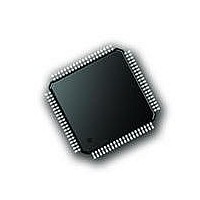
PIC18F87J72-I/PT Microchip Technology, PIC18F87J72-I/PT Datasheet - Page 168

PIC18F87J72-I/PT
Manufacturer Part Number
PIC18F87J72-I/PT
Description
IC PIC MCU 8BIT 14KB FLSH 80TQFP
Manufacturer
Microchip Technology
Series
PIC® 18Fr
Datasheet
1.PIC18F86J72-IPT.pdf
(480 pages)
Specifications of PIC18F87J72-I/PT
Program Memory Type
FLASH
Program Memory Size
128KB (64K x 16)
Package / Case
80-TQFP
Core Processor
PIC
Core Size
8-Bit
Speed
48MHz
Connectivity
I²C, LIN, SPI, UART/USART
Peripherals
Brown-out Detect/Reset, LCD, LVD, POR, PWM, WDT
Number Of I /o
51
Ram Size
3.8K x 8
Voltage - Supply (vcc/vdd)
2 V ~ 3.6 V
Data Converters
A/D 12x12b
Oscillator Type
Internal
Operating Temperature
-40°C ~ 85°C
Data Bus Width
8 bit
Data Ram Size
4 KB
Interface Type
SPI, USART, SPI, I2C
Maximum Clock Frequency
8 MHz
Number Of Programmable I/os
51
Number Of Timers
4
Operating Supply Voltage
2 V to 3.6 V
Maximum Operating Temperature
+ 85 C
Mounting Style
SMD/SMT
Minimum Operating Temperature
- 40 C
On-chip Adc
14
Controller Family/series
PIC18F
No. Of I/o's
51
Ram Memory Size
3923Byte
Cpu Speed
48MHz
No. Of Timers
4
Rohs Compliant
Yes
Lead Free Status / RoHS Status
Lead free / RoHS Compliant
Lead Free Status / RoHS Status
Lead free / RoHS Compliant, Lead free / RoHS Compliant
Available stocks
Company
Part Number
Manufacturer
Quantity
Price
Company:
Part Number:
PIC18F87J72-I/PT
Manufacturer:
Microchip
Quantity:
210
Company:
Part Number:
PIC18F87J72-I/PT
Manufacturer:
Microchip Technology
Quantity:
10 000
- Current page: 168 of 480
- Download datasheet (5Mb)
PIC18F87J72 FAMILY
17.1
The LCD driver module has 33 registers:
• LCD Control Register (LCDCON)
• LCD Phase Register (LCDPS)
• LCDREG Register (LCD Regulator Control)
• Five LCD Segment Enable Registers
• 20 LCD Data Registers (LCDDATAx, for x from 0 to
17.1.1
The LCDCON register, shown in Register 17-1,
controls the overall operation of the module. Once the
module is configured, the LCDEN (LCDCON<7>) bit is
used to enable or disable the LCD module. The LCD
panel can also operate during Sleep by clearing the
SLPEN (LCDCON<6>) bit.
REGISTER 17-1:
DS39979A-page 168
bit 7
Legend:
R = Readable bit
-n = Value at POR
bit 7
bit 6
bit 5
bit 4
bit 3-2
bit 1-0
(LCDSE4:LCDSE0)
22, with 5, 11 and 17 not implemented)
LCDEN
R/W-0
LCD Registers
LCD CONTROL REGISTERS
LCDEN: LCD Driver Enable bit
1 = LCD driver module is enabled
0 = LCD driver module is disabled
SLPEN: LCD Driver Enable in Sleep mode bit
1 = LCD driver module is disabled in Sleep mode
0 = LCD driver module is enabled in Sleep mode
WERR: LCD Write Failed Error bit
1 = LCDDATAx register written while LCDPS<4> = 0 (must be cleared in software)
0 = No LCD write error
Unimplemented: Read as ‘0’
CS<1:0>: Clock Source Select bits
1x = INTRC (31 kHz)
01 = T13CKI (Timer1)
00 = System clock (F
LMUX<1:0>: Commons Select bits
SLPEN
R/W-0
LMUX<1:0>
LCDCON: LCD CONTROL REGISTER
00
01
10
11
C = Clearable bit
W = Writable bit
‘1’ = Bit is set
WERR
R/C-0
OSC
1/2 (COM1:COM0)
1/3 (COM2:COM0)
1/4 (COM3:COM0)
/4)
Multiplex Type
Static (COM0)
U-0
—
Preliminary
U = Unimplemented bit, read as ‘0’
‘0’ = Bit is cleared
R/W-0
The
configures the LCD clock source prescaler and the type
of waveform: Type-A or Type-B. Details on these
features are provided in Section 17.2 “LCD Clock
Source”, Section 17.3 “LCD Bias Generation” and
Section 17.8 “LCD Waveform Generation”.
The LCDREG register is described in Section 17.3
“LCD Bias Generation”.
The LCD Segment Enable registers (LCDSEx)
configure the functions of the port pins. Setting the
segment enable bit for a particular segment configures
that pin as an LCD driver. The prototype LCDSE
register is shown in Register 17-3. There are five
LCDSE
Table 17-1.
Maximum Number
CS1
of Pixels
LCDPS
132
33
66
99
registers
R/W-0
CS0
register,
(LCDSE4:LCDSE0),
2010 Microchip Technology Inc.
x = Bit is unknown
shown
Bias Type
1/2 or 1/3
1/2 or 1/3
LMUX1
R/W-0
Static
1/3
in
Register 17-2,
LMUX0
R/W-0
listed
bit 0
in
Related parts for PIC18F87J72-I/PT
Image
Part Number
Description
Manufacturer
Datasheet
Request
R

Part Number:
Description:
Manufacturer:
Microchip Technology Inc.
Datasheet:

Part Number:
Description:
Manufacturer:
Microchip Technology Inc.
Datasheet:

Part Number:
Description:
Manufacturer:
Microchip Technology Inc.
Datasheet:

Part Number:
Description:
Manufacturer:
Microchip Technology Inc.
Datasheet:

Part Number:
Description:
Manufacturer:
Microchip Technology Inc.
Datasheet:

Part Number:
Description:
Manufacturer:
Microchip Technology Inc.
Datasheet:

Part Number:
Description:
Manufacturer:
Microchip Technology Inc.
Datasheet:

Part Number:
Description:
Manufacturer:
Microchip Technology Inc.
Datasheet:


