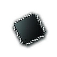
PIC18F87J72-I/PT Microchip Technology, PIC18F87J72-I/PT Datasheet - Page 443

PIC18F87J72-I/PT
Manufacturer Part Number
PIC18F87J72-I/PT
Description
IC PIC MCU 8BIT 14KB FLSH 80TQFP
Manufacturer
Microchip Technology
Series
PIC® 18Fr
Datasheet
1.PIC18F86J72-IPT.pdf
(480 pages)
Specifications of PIC18F87J72-I/PT
Program Memory Type
FLASH
Program Memory Size
128KB (64K x 16)
Package / Case
80-TQFP
Core Processor
PIC
Core Size
8-Bit
Speed
48MHz
Connectivity
I²C, LIN, SPI, UART/USART
Peripherals
Brown-out Detect/Reset, LCD, LVD, POR, PWM, WDT
Number Of I /o
51
Ram Size
3.8K x 8
Voltage - Supply (vcc/vdd)
2 V ~ 3.6 V
Data Converters
A/D 12x12b
Oscillator Type
Internal
Operating Temperature
-40°C ~ 85°C
Data Bus Width
8 bit
Data Ram Size
4 KB
Interface Type
SPI, USART, SPI, I2C
Maximum Clock Frequency
8 MHz
Number Of Programmable I/os
51
Number Of Timers
4
Operating Supply Voltage
2 V to 3.6 V
Maximum Operating Temperature
+ 85 C
Mounting Style
SMD/SMT
Minimum Operating Temperature
- 40 C
On-chip Adc
14
Controller Family/series
PIC18F
No. Of I/o's
51
Ram Memory Size
3923Byte
Cpu Speed
48MHz
No. Of Timers
4
Rohs Compliant
Yes
Lead Free Status / RoHS Status
Lead free / RoHS Compliant
Lead Free Status / RoHS Status
Lead free / RoHS Compliant, Lead free / RoHS Compliant
Available stocks
Company
Part Number
Manufacturer
Quantity
Price
Company:
Part Number:
PIC18F87J72-I/PT
Manufacturer:
Microchip
Quantity:
210
Company:
Part Number:
PIC18F87J72-I/PT
Manufacturer:
Microchip Technology
Quantity:
10 000
- Current page: 443 of 480
- Download datasheet (5Mb)
When an ADC exits ADC Shutdown mode, any phase
delay present before shutdown was entered will still be
present. If one ADC was not in shutdown, the ADC
leaving
automatically the phase delay relative to the other ADC
channel per the Phase Delay register block and give
DR pulses accordingly.
If an ADC is placed in Shutdown mode while the other
is converting, it is not shutting down the internal clock.
When going back out of shutdown, it will be
resynchronized automatically with the clock that did not
stop during Reset.
If both ADCs are in ADC Reset or ADC Shutdown
modes, the clock is no more distributed to the digital
core for low-power operation. Once any of the ADC is
back to normal operation, the clock is automatically
distributed again.
B.3.21
The lowest power consumption can be achieved when
SHUTDOWN<1:0> = 11, VREFEXT = CLKEXT = 1.
This mode is called “Full Shutdown mode” and no ana-
log circuitry is enabled. In this mode, the POR SV
monitoring circuit is also disabled. When the clock is
Idle (CLKIA = 0 or 1 continuously), no clock is propa-
gated throughout the chip. Both ADCs are in shutdown,
the internal voltage reference is disabled and the
internal oscillator is disabled.
The only circuit that remains active is the SPI interface,
but this circuit does not induce any static power
consumption. If SCK is Idle, the only current
consumption comes from the leakage currents induced
by the transistors and is less than 1 µA on each power
supply.
This mode can be used to power down the chip
completely and avoid power consumption when there
is no data to convert at the analog inputs. Any SCK or
MCLK edge coming, while on this mode, will induce
dynamic power consumption.
Once any of the SHUTDOWN, CLKEXT and VREFEXT
bits returns to ‘0’, the POR SV
back to operation and SV
2010 Microchip Technology Inc.
Shutdown
FULL SHUTDOWN MODE
mode
DD
monitoring can take place.
DD
will
monitoring block is
resynchronize
Preliminary
DD
PIC18F87J72 FAMILY
B.4
B.4.1
The analog inputs of the dual-channel AFE can be con-
nected directly to current and voltage transducers (such
as shunts, current transformers or Rogowski coils). Each
input pin is protected by specialized ESD structures that
are certified to pass 7 kV HBM and 400V MM contact
charge. These structures allow bipolar ±6V continuous
voltage, with respect to SAV
inputs without the risk of permanent damage.
Both channels have fully differential voltage inputs for
better noise performance. The absolute voltage at each
pin relative to SAV
range during operation in order to ensure the specified
ADC accuracy. The common-mode signals should be
adapted to respect both the previous conditions and
the
performance, the common-mode signals should be
maintained to SAV
B.4.2
The two Programmable Gain Amplifiers (PGAs) reside
at the front end of each Delta-Sigma ADC. They have
two functions: translate the common-mode of the input
from SAV
SAV
translation of the common-mode does not change the
differential signal, but re-centers the common-mode so
that the input signal can be properly amplified.
The PGA block can be used to amplify very low signals,
but the differential input range of the Delta-Sigma
modulator must not be exceeded. The PGA is
controlled by the
register. Table B-4 represents the gain settings for the
PGA:
TABLE B-4:
(PGA_CHn<2:0>)
0
0
0
0
1
1
DD
PGA Gain
differential
, and amplify the input differential signal. The
Device Overview
SS
0
0
1
1
0
0
ANALOG INPUTS (CHn+/-)
PROGRAMMABLE GAIN
AMPLIFIERS (PGA)
to an internal level between SAV
0
1
0
1
0
1
PGA CONFIGURATION
SETTING
PGA_CHn<2:0>
input
SS
SS
.
should be maintained in the ±1V
(V/V)
16
32
1
2
4
8
voltage
Gain
SS
, to be present at their
(dB)
12
18
24
30
0
6
range.
DS39979A-page 443
bits in the GAIN
±0.5
±0.25
±0.125
±0.0625
±0.03125
±0.015625
V
IN
For
Range
(V)
SS
best
and
Related parts for PIC18F87J72-I/PT
Image
Part Number
Description
Manufacturer
Datasheet
Request
R

Part Number:
Description:
Manufacturer:
Microchip Technology Inc.
Datasheet:

Part Number:
Description:
Manufacturer:
Microchip Technology Inc.
Datasheet:

Part Number:
Description:
Manufacturer:
Microchip Technology Inc.
Datasheet:

Part Number:
Description:
Manufacturer:
Microchip Technology Inc.
Datasheet:

Part Number:
Description:
Manufacturer:
Microchip Technology Inc.
Datasheet:

Part Number:
Description:
Manufacturer:
Microchip Technology Inc.
Datasheet:

Part Number:
Description:
Manufacturer:
Microchip Technology Inc.
Datasheet:

Part Number:
Description:
Manufacturer:
Microchip Technology Inc.
Datasheet:


