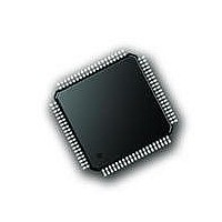
PIC18F87J72-I/PT Microchip Technology, PIC18F87J72-I/PT Datasheet - Page 173

PIC18F87J72-I/PT
Manufacturer Part Number
PIC18F87J72-I/PT
Description
IC PIC MCU 8BIT 14KB FLSH 80TQFP
Manufacturer
Microchip Technology
Series
PIC® 18Fr
Datasheet
1.PIC18F86J72-IPT.pdf
(480 pages)
Specifications of PIC18F87J72-I/PT
Program Memory Type
FLASH
Program Memory Size
128KB (64K x 16)
Package / Case
80-TQFP
Core Processor
PIC
Core Size
8-Bit
Speed
48MHz
Connectivity
I²C, LIN, SPI, UART/USART
Peripherals
Brown-out Detect/Reset, LCD, LVD, POR, PWM, WDT
Number Of I /o
51
Ram Size
3.8K x 8
Voltage - Supply (vcc/vdd)
2 V ~ 3.6 V
Data Converters
A/D 12x12b
Oscillator Type
Internal
Operating Temperature
-40°C ~ 85°C
Data Bus Width
8 bit
Data Ram Size
4 KB
Interface Type
SPI, USART, SPI, I2C
Maximum Clock Frequency
8 MHz
Number Of Programmable I/os
51
Number Of Timers
4
Operating Supply Voltage
2 V to 3.6 V
Maximum Operating Temperature
+ 85 C
Mounting Style
SMD/SMT
Minimum Operating Temperature
- 40 C
On-chip Adc
14
Controller Family/series
PIC18F
No. Of I/o's
51
Ram Memory Size
3923Byte
Cpu Speed
48MHz
No. Of Timers
4
Rohs Compliant
Yes
Lead Free Status / RoHS Status
Lead free / RoHS Compliant
Lead Free Status / RoHS Status
Lead free / RoHS Compliant, Lead free / RoHS Compliant
Available stocks
Company
Part Number
Manufacturer
Quantity
Price
Company:
Part Number:
PIC18F87J72-I/PT
Manufacturer:
Microchip
Quantity:
210
Company:
Part Number:
PIC18F87J72-I/PT
Manufacturer:
Microchip Technology
Quantity:
10 000
- Current page: 173 of 480
- Download datasheet (5Mb)
17.3
The LCD driver module is capable of generating the
required bias voltages for LCD operation with a mini-
mum of external components. This includes the ability
to generate the different voltage levels required by the
different bias types required by the LCD. The driver
module can also provide bias voltages both above and
below microcontroller V
on-chip LCD voltage regulator.
17.3.1
PIC18F87J72 family devices support three bias types
based on the waveforms generated to control
segments and commons:
• Static (two discrete levels)
• 1/2 Bias (three discrete levels
• 1/3 Bias (four discrete levels)
The use of different waveforms in driving the LCD is dis-
cussed in more detail in Section 17.8 “LCD Waveform
Generation”.
REGISTER 17-5:
2010 Microchip Technology Inc.
bit 7
Legend:
R = Readable bit
-n = Value at POR
bit 7
bit 6
bit 5-3
bit 2
bit 1-0
U-0
—
LCD Bias Generation
LCD BIAS TYPES
Unimplemented: Read as ‘0’
CPEN: LCD Charge Pump Enable bit
1 = Charge pump enabled; highest LCD bias voltage is 3.6V
0 = Charge pump disabled; highest LCD bias voltage is AV
BIAS<2:0>: Regulator Voltage Output Control bits
111 = 3.60V peak (offset on LCDBIAS0 of 0V)
110 = 3.47V peak (offset on LCDBIAS0 of 0.13V)
101 = 3.34V peak (offset on LCDBIAS0 of 0.26V)
100 = 3.21V peak (offset on LCDBIAS0 of 0.39V)
011 = 3.08V peak (offset on LCDBIAS0 of 0.52V)
010 = 2.95V peak (offset on LCDBIAS0 of 0.65V)
001 = 2.82V peak (offset on LCDBIAS0 of 0.78V)
000 = 2.69V peak (offset on LCDBIAS0 of 0.91V)
MODE13: 1/3 LCD Bias Enable bit
1 = Regulator output supports 1/3 LCD Bias mode
0 = Regulator output supports Static LCD Bias mode
CKSEL<1:0>: Regulator Clock Source Select bits
11 = INTRC
10 = INTOSC 8 MHz source
01 = Timer1 oscillator
00 = LCD regulator disabled
CPEN
RW-0
LCDREG: VOLTAGE REGULATOR CONTROL REGISTER
DD
through the use of an
W = Writable bit
‘1’ = Bit is set
BIAS2
RW-1
BIAS1
RW-1
Preliminary
U = Unimplemented bit, read as ‘0’
‘0’ = Bit is cleared
PIC18F87J72 FAMILY
BIAS0
17.3.2
The purpose of the LCD regulator is to provide proper
bias voltage and good contrast for the LCD, regardless
of V
internal voltage reference. The regulator can be config-
ured by using external components to boost bias
voltage above V
constant voltage below V
selectively disabled to allow bias voltages to be
generated by an external resistor network.
The LCD regulator is controlled through the LCDREG
register (Register 17-5). It is enabled or disabled using
the CKSEL<1:0> bits, while the charge pump can be
selectively enabled using the CPEN bit. When the reg-
ulator is enabled, the MODE13 bit is used to select the
bias type. The peak LCD bias voltage, measured as a
difference between the potentials of LCDBIAS3 and
LCDBIAS0, is configured with the BIAS bits.
RW-1
DD
levels. This module contains a charge pump and
DD
LCD VOLTAGE REGULATOR
MODE13
RW-1
DD
. It can also operate a display at a
DD
x = Bit is unknown
. The regulator can also be
CKSEL1
RW-0
DS39979A-page 173
CKSEL0
RW-0
bit 0
Related parts for PIC18F87J72-I/PT
Image
Part Number
Description
Manufacturer
Datasheet
Request
R

Part Number:
Description:
Manufacturer:
Microchip Technology Inc.
Datasheet:

Part Number:
Description:
Manufacturer:
Microchip Technology Inc.
Datasheet:

Part Number:
Description:
Manufacturer:
Microchip Technology Inc.
Datasheet:

Part Number:
Description:
Manufacturer:
Microchip Technology Inc.
Datasheet:

Part Number:
Description:
Manufacturer:
Microchip Technology Inc.
Datasheet:

Part Number:
Description:
Manufacturer:
Microchip Technology Inc.
Datasheet:

Part Number:
Description:
Manufacturer:
Microchip Technology Inc.
Datasheet:

Part Number:
Description:
Manufacturer:
Microchip Technology Inc.
Datasheet:


