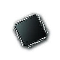
PIC18F87J72-I/PT Microchip Technology, PIC18F87J72-I/PT Datasheet - Page 136

PIC18F87J72-I/PT
Manufacturer Part Number
PIC18F87J72-I/PT
Description
IC PIC MCU 8BIT 14KB FLSH 80TQFP
Manufacturer
Microchip Technology
Series
PIC® 18Fr
Datasheet
1.PIC18F86J72-IPT.pdf
(480 pages)
Specifications of PIC18F87J72-I/PT
Program Memory Type
FLASH
Program Memory Size
128KB (64K x 16)
Package / Case
80-TQFP
Core Processor
PIC
Core Size
8-Bit
Speed
48MHz
Connectivity
I²C, LIN, SPI, UART/USART
Peripherals
Brown-out Detect/Reset, LCD, LVD, POR, PWM, WDT
Number Of I /o
51
Ram Size
3.8K x 8
Voltage - Supply (vcc/vdd)
2 V ~ 3.6 V
Data Converters
A/D 12x12b
Oscillator Type
Internal
Operating Temperature
-40°C ~ 85°C
Data Bus Width
8 bit
Data Ram Size
4 KB
Interface Type
SPI, USART, SPI, I2C
Maximum Clock Frequency
8 MHz
Number Of Programmable I/os
51
Number Of Timers
4
Operating Supply Voltage
2 V to 3.6 V
Maximum Operating Temperature
+ 85 C
Mounting Style
SMD/SMT
Minimum Operating Temperature
- 40 C
On-chip Adc
14
Controller Family/series
PIC18F
No. Of I/o's
51
Ram Memory Size
3923Byte
Cpu Speed
48MHz
No. Of Timers
4
Rohs Compliant
Yes
Lead Free Status / RoHS Status
Lead free / RoHS Compliant
Lead Free Status / RoHS Status
Lead free / RoHS Compliant, Lead free / RoHS Compliant
Available stocks
Company
Part Number
Manufacturer
Quantity
Price
Company:
Part Number:
PIC18F87J72-I/PT
Manufacturer:
Microchip
Quantity:
210
Company:
Part Number:
PIC18F87J72-I/PT
Manufacturer:
Microchip Technology
Quantity:
10 000
- Current page: 136 of 480
- Download datasheet (5Mb)
PIC18F87J72 FAMILY
14.1
Timer3 can operate in one of three modes:
• Timer
• Synchronous Counter
• Asynchronous Counter
FIGURE 14-1:
FIGURE 14-2:
DS39979A-page 136
Note 1: When enable bit, T1OSCEN, is cleared, the inverter and feedback resistor are turned off to eliminate power drain.
Note 1: When enable bit, T1OSCEN, is cleared, the inverter and feedback resistor are turned off to eliminate power drain.
T1OSO/T13CKI
T13CKI/T1OSO
Timer3 Operation
T1OSI
T1OSI
CCPx Select from T3CON<6,3>
CCPx Select from T3CON<6,3>
Timer1 Oscillator
Timer1 Oscillator
CCPx Special Event Trigger
T1OSCEN
T3CKPS<1:0>
T3SYNC
TMR3ON
TIMER3 BLOCK DIAGRAM (8-BIT MODE)
T1OSCEN
T3CKPS<1:0>
T3SYNC
TMR3ON
CCPx Special Event Trigger
TIMER3 BLOCK DIAGRAM (16-BIT READ/WRITE MODE)
(1)
(1)
TMR3CS
TMR3CS
Clock
Internal
F
Internal
Clock
F
OSC
OSC
/4
/4
Preliminary
1
0
1
0
Timer1 Clock Input
Timer1 Clock Input
Clear TMR3
Clear TMR3
Prescaler
Prescaler
1, 2, 4, 8
1, 2, 4, 8
The operating mode is determined by the clock select
bit, TMR3CS (T3CON<1>). When TMR3CS is cleared
(= 0), Timer3 increments on every internal instruction
cycle (F
on every rising edge of the Timer1 external clock input
or the Timer1 oscillator, if enabled.
As
RC0/T1OSO/T13CKI pins become inputs when the
Timer1 oscillator is enabled. This means the values of
TRISC<1:0> are ignored and the pins are read as ‘0’.
2
2
with
OSC
TMR3L
TMR3L
Timer1,
/4). When the bit is set, Timer3 increments
8
8
Synchronize
Synchronize
Sleep Input
Sleep Input
Detect
Detect
High Byte
High Byte
the
TMR3H
TMR3
TMR3
8
2010 Microchip Technology Inc.
8
RC1/T1OSI/SEG32
8
Internal Data Bus
1
0
1
0
Read TMR3L
Write TMR3L
Set
TMR3IF
on Overflow
Set
TMR3IF
on Overflow
Timer3
On/Off
Timer3
On/Off
and
Related parts for PIC18F87J72-I/PT
Image
Part Number
Description
Manufacturer
Datasheet
Request
R

Part Number:
Description:
Manufacturer:
Microchip Technology Inc.
Datasheet:

Part Number:
Description:
Manufacturer:
Microchip Technology Inc.
Datasheet:

Part Number:
Description:
Manufacturer:
Microchip Technology Inc.
Datasheet:

Part Number:
Description:
Manufacturer:
Microchip Technology Inc.
Datasheet:

Part Number:
Description:
Manufacturer:
Microchip Technology Inc.
Datasheet:

Part Number:
Description:
Manufacturer:
Microchip Technology Inc.
Datasheet:

Part Number:
Description:
Manufacturer:
Microchip Technology Inc.
Datasheet:

Part Number:
Description:
Manufacturer:
Microchip Technology Inc.
Datasheet:


