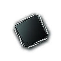
PIC18F87J72-I/PT Microchip Technology, PIC18F87J72-I/PT Datasheet - Page 389

PIC18F87J72-I/PT
Manufacturer Part Number
PIC18F87J72-I/PT
Description
IC PIC MCU 8BIT 14KB FLSH 80TQFP
Manufacturer
Microchip Technology
Series
PIC® 18Fr
Datasheet
1.PIC18F86J72-IPT.pdf
(480 pages)
Specifications of PIC18F87J72-I/PT
Program Memory Type
FLASH
Program Memory Size
128KB (64K x 16)
Package / Case
80-TQFP
Core Processor
PIC
Core Size
8-Bit
Speed
48MHz
Connectivity
I²C, LIN, SPI, UART/USART
Peripherals
Brown-out Detect/Reset, LCD, LVD, POR, PWM, WDT
Number Of I /o
51
Ram Size
3.8K x 8
Voltage - Supply (vcc/vdd)
2 V ~ 3.6 V
Data Converters
A/D 12x12b
Oscillator Type
Internal
Operating Temperature
-40°C ~ 85°C
Data Bus Width
8 bit
Data Ram Size
4 KB
Interface Type
SPI, USART, SPI, I2C
Maximum Clock Frequency
8 MHz
Number Of Programmable I/os
51
Number Of Timers
4
Operating Supply Voltage
2 V to 3.6 V
Maximum Operating Temperature
+ 85 C
Mounting Style
SMD/SMT
Minimum Operating Temperature
- 40 C
On-chip Adc
14
Controller Family/series
PIC18F
No. Of I/o's
51
Ram Memory Size
3923Byte
Cpu Speed
48MHz
No. Of Timers
4
Rohs Compliant
Yes
Lead Free Status / RoHS Status
Lead free / RoHS Compliant
Lead Free Status / RoHS Status
Lead free / RoHS Compliant, Lead free / RoHS Compliant
Available stocks
Company
Part Number
Manufacturer
Quantity
Price
Company:
Part Number:
PIC18F87J72-I/PT
Manufacturer:
Microchip
Quantity:
210
Company:
Part Number:
PIC18F87J72-I/PT
Manufacturer:
Microchip Technology
Quantity:
10 000
- Current page: 389 of 480
- Download datasheet (5Mb)
29.0
Absolute Maximum Ratings
Ambient temperature under bias.............................................................................................................-40°C to +100°C
Storage temperature .............................................................................................................................. -65°C to +150°C
Voltage on any digital only I/O pin or MCLR with respect to V
Voltage on any combined digital and analog pin with respect to V
Voltage on V
Voltage on V
Total power dissipation (Note 1) ...............................................................................................................................1.0W
Maximum current out of V
Maximum current into V
Maximum output current sunk by PORTA<7:6> and any PORTB and PORTC I/O pins.........................................25 mA
Maximum output current sunk by any PORTD, PORTE and PORTJ I/O pins ..........................................................8 mA
Maximum output current sunk by PORTA<5:0> and any PORTF, PORTG and PORTH I/O pins ............................2 mA
Maximum output current sourced by PORTA<7:6> and any PORTB and PORTC I/O pins ...................................25 mA
Maximum output current sourced by any PORTD, PORTE and PORTJ I/O pins .....................................................8 mA
Maximum output current sourced by PORTA<5:0> and any PORTF, PORTG and PORTH I/O pins .......................2 mA
Maximum current sunk byall ports combined.......................................................................................................200 mA
Voltage on AFE SV
AFE digital inputs and outputs with respect to SAV
AFE analog input with respect to SAV
AFE V
ESD on the AFE analog inputs (HBM
ESD on all other AFE pins (HBM
2010 Microchip Technology Inc.
† NOTICE: Stresses above those listed under “Absolute Maximum Ratings” may cause permanent damage to the
device. This is a stress rating only and functional operation of the device at those or any other conditions above those
indicated in the operation listings of this specification is not implied. Exposure to maximum rating conditions for
extended periods may affect device reliability.
Note 1: Power dissipation is calculated as follows:
REF
2: Human Body Model for ESD testing.
3: Machine Model for ESD testing.
ELECTRICAL CHARACTERISTICS
input with respect to SAV
Pdis = V
DDCORE
DD
with respect to V
DD
DD
with respect to V
................................................................................................................................................7.0V
x {I
DD
SS
DD
pin ..............................................................................................................................250 mA
pin ...........................................................................................................................300 mA
– I
SS
(2)
OH
,MM
SS
(†)
........................................................................................................... -0.3V to 3.6V
(2)
} + {(V
SS
SS
.........................................................................................-0.6V to (SV
,MM
(3)
...................................................................................................... ....-6V to +6V
................................................................................................... -0.3V to 2.75V
) ................................................................................................... 7.0 kV, 400V
(3)
) ............................................................................................ 7.0 kV, 400V
DD
– V
SS
Preliminary
OH
..................................................................-0.6V to (SV
) x I
OH
SS
PIC18F87J72 FAMILY
} + (V
(except V
SS
(except V
OL
x I
DD
OL
) ........................................... -0.3V to 5.6V
)
DD
and MCLR)...... -0.3V to (V
DS39979A-page 389
DD
DD
DD
+ 0.3V)
+ 0.6V)
+ 0.6V)
Related parts for PIC18F87J72-I/PT
Image
Part Number
Description
Manufacturer
Datasheet
Request
R

Part Number:
Description:
Manufacturer:
Microchip Technology Inc.
Datasheet:

Part Number:
Description:
Manufacturer:
Microchip Technology Inc.
Datasheet:

Part Number:
Description:
Manufacturer:
Microchip Technology Inc.
Datasheet:

Part Number:
Description:
Manufacturer:
Microchip Technology Inc.
Datasheet:

Part Number:
Description:
Manufacturer:
Microchip Technology Inc.
Datasheet:

Part Number:
Description:
Manufacturer:
Microchip Technology Inc.
Datasheet:

Part Number:
Description:
Manufacturer:
Microchip Technology Inc.
Datasheet:

Part Number:
Description:
Manufacturer:
Microchip Technology Inc.
Datasheet:


