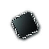
PIC18F87J72-I/PT Microchip Technology, PIC18F87J72-I/PT Datasheet - Page 450

PIC18F87J72-I/PT
Manufacturer Part Number
PIC18F87J72-I/PT
Description
IC PIC MCU 8BIT 14KB FLSH 80TQFP
Manufacturer
Microchip Technology
Series
PIC® 18Fr
Datasheet
1.PIC18F86J72-IPT.pdf
(480 pages)
Specifications of PIC18F87J72-I/PT
Program Memory Type
FLASH
Program Memory Size
128KB (64K x 16)
Package / Case
80-TQFP
Core Processor
PIC
Core Size
8-Bit
Speed
48MHz
Connectivity
I²C, LIN, SPI, UART/USART
Peripherals
Brown-out Detect/Reset, LCD, LVD, POR, PWM, WDT
Number Of I /o
51
Ram Size
3.8K x 8
Voltage - Supply (vcc/vdd)
2 V ~ 3.6 V
Data Converters
A/D 12x12b
Oscillator Type
Internal
Operating Temperature
-40°C ~ 85°C
Data Bus Width
8 bit
Data Ram Size
4 KB
Interface Type
SPI, USART, SPI, I2C
Maximum Clock Frequency
8 MHz
Number Of Programmable I/os
51
Number Of Timers
4
Operating Supply Voltage
2 V to 3.6 V
Maximum Operating Temperature
+ 85 C
Mounting Style
SMD/SMT
Minimum Operating Temperature
- 40 C
On-chip Adc
14
Controller Family/series
PIC18F
No. Of I/o's
51
Ram Memory Size
3923Byte
Cpu Speed
48MHz
No. Of Timers
4
Rohs Compliant
Yes
Lead Free Status / RoHS Status
Lead free / RoHS Compliant
Lead Free Status / RoHS Status
Lead free / RoHS Compliant, Lead free / RoHS Compliant
Available stocks
Company
Part Number
Manufacturer
Quantity
Price
Company:
Part Number:
PIC18F87J72-I/PT
Manufacturer:
Microchip
Quantity:
210
Company:
Part Number:
PIC18F87J72-I/PT
Manufacturer:
Microchip Technology
Quantity:
10 000
- Current page: 450 of 480
- Download datasheet (5Mb)
PIC18F87J72 FAMILY
B.5.3
The first data byte read is the one defined by the
address given in the control byte. After this first byte is
transmitted, if the CS pin is maintained low, the com-
munication continues and the address of the next
transmitted byte is determined by the status of the
READ bits in the STATUS/COM register. Multiple
looping configurations can be defined through the
READ<1:0> bits for the address increment (see
Section B.5.6 “SPI Mode 0,0 - Clock Idle Low,
Read/Write Examples”).
B.5.4
The first data byte written is the one defined by the
address given in the control byte. The write
communication automatically increments the address
for subsequent bytes.
FIGURE B-7:
FIGURE B-8:
DS39979A-page 450
CS
SCK
SDI
SDO
CS
SCK
SDI
SDO
Bits on the Rising Edge
Bits on the Rising Edge
WRITING TO THE DEVICE
READING FROM THE DEVICE
Data Transitions on
HI-Z
Data Transitions on
the Falling Edge
HI-Z
the Falling Edge
AFE Latches
DEVICE READ (SPI MODE 1,1 – CLOCK IDLES HIGH)
DEVICE WRITE (SPI MODE 1,1 – CLOCK IDLES HIGH)
AFE Latches
A6 A5 A4 A3 A2 A1 A0
A6 A5 A4 A3 A2 A1
HI-Z
R/W
A0
R/W
(ADDRESS) DATA
(ADDRESS) DATA
Preliminary
D7
D7 D6 D5 D4 D3 D2 D1
D6 D5 D4 D3 D2 D1
HI-Z
The address of the next transmitted byte within the
same communication (CSA stays low) is the next
address defined on the register map. At the end of the
register map, the address loops to the beginning of the
register map. Writing a non-writable register has no
effect.
The SDOA pin stays in a high-impedance state during
a write communication.
B.5.5
In this SPI mode, the clock Idles high. For the AFE, this
means that there will be a falling edge before there is a
rising edge.
Note:
D0
D0
(ADDRESS + 1) DATA
SPI MODE 1,1 – CLOCK IDLE HIGH,
READ/WRITE EXAMPLES
Changing from an SPI Mode 1,1 to an SPI
Mode 0,0 is possible, but needs a Reset
pulse
communication.
D7
(ADDRESS + 1) DATA
D6 D5 D4 D3 D2 D1
D7
D6 D5 D4 D3 D2
in-between
2010 Microchip Technology Inc.
D1
D0
D0
to
ensure
HI-Z
correct
HI-Z
Related parts for PIC18F87J72-I/PT
Image
Part Number
Description
Manufacturer
Datasheet
Request
R

Part Number:
Description:
Manufacturer:
Microchip Technology Inc.
Datasheet:

Part Number:
Description:
Manufacturer:
Microchip Technology Inc.
Datasheet:

Part Number:
Description:
Manufacturer:
Microchip Technology Inc.
Datasheet:

Part Number:
Description:
Manufacturer:
Microchip Technology Inc.
Datasheet:

Part Number:
Description:
Manufacturer:
Microchip Technology Inc.
Datasheet:

Part Number:
Description:
Manufacturer:
Microchip Technology Inc.
Datasheet:

Part Number:
Description:
Manufacturer:
Microchip Technology Inc.
Datasheet:

Part Number:
Description:
Manufacturer:
Microchip Technology Inc.
Datasheet:


