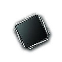
PIC18F87J72-I/PT Microchip Technology, PIC18F87J72-I/PT Datasheet - Page 196

PIC18F87J72-I/PT
Manufacturer Part Number
PIC18F87J72-I/PT
Description
IC PIC MCU 8BIT 14KB FLSH 80TQFP
Manufacturer
Microchip Technology
Series
PIC® 18Fr
Datasheet
1.PIC18F86J72-IPT.pdf
(480 pages)
Specifications of PIC18F87J72-I/PT
Program Memory Type
FLASH
Program Memory Size
128KB (64K x 16)
Package / Case
80-TQFP
Core Processor
PIC
Core Size
8-Bit
Speed
48MHz
Connectivity
I²C, LIN, SPI, UART/USART
Peripherals
Brown-out Detect/Reset, LCD, LVD, POR, PWM, WDT
Number Of I /o
51
Ram Size
3.8K x 8
Voltage - Supply (vcc/vdd)
2 V ~ 3.6 V
Data Converters
A/D 12x12b
Oscillator Type
Internal
Operating Temperature
-40°C ~ 85°C
Data Bus Width
8 bit
Data Ram Size
4 KB
Interface Type
SPI, USART, SPI, I2C
Maximum Clock Frequency
8 MHz
Number Of Programmable I/os
51
Number Of Timers
4
Operating Supply Voltage
2 V to 3.6 V
Maximum Operating Temperature
+ 85 C
Mounting Style
SMD/SMT
Minimum Operating Temperature
- 40 C
On-chip Adc
14
Controller Family/series
PIC18F
No. Of I/o's
51
Ram Memory Size
3923Byte
Cpu Speed
48MHz
No. Of Timers
4
Rohs Compliant
Yes
Lead Free Status / RoHS Status
Lead free / RoHS Compliant
Lead Free Status / RoHS Status
Lead free / RoHS Compliant, Lead free / RoHS Compliant
Available stocks
Company
Part Number
Manufacturer
Quantity
Price
Company:
Part Number:
PIC18F87J72-I/PT
Manufacturer:
Microchip
Quantity:
210
Company:
Part Number:
PIC18F87J72-I/PT
Manufacturer:
Microchip Technology
Quantity:
10 000
- Current page: 196 of 480
- Download datasheet (5Mb)
PIC18F87J72 FAMILY
18.3.1
Each MSSP module has four registers for SPI mode
operation. These are:
• MSSP Control Register 1 (SSPCON1)
• MSSP Status Register (SSPSTAT)
• Serial Receive/Transmit Buffer Register (SSPBUF)
• MSSP Shift Register (SSPSR) – Not directly
SSPCON1 and SSPSTAT are the control and status
registers in SPI mode operation. The SSPCON1
register is readable and writable. The lower 6 bits of
the SSPSTAT are read-only. The upper two bits of the
SSPSTAT are read/write.
REGISTER 18-1:
DS39979A-page 196
bit 7
Legend:
R = Readable bit
-n = Value at POR
bit 7
bit 6
bit 5
bit 4
bit 3
bit 2
bit 1
bit 0
Note 1:
accessible
R/W-0
SMP
Polarity of clock state is set by the CKP bit (SSPCON1<4>).
REGISTERS
SMP: Sample bit
SPI Master mode:
1 = Input data sampled at end of data output time
0 = Input data sampled at middle of data output time
SPI Slave mode:
SMP must be cleared when SPI is used in Slave mode.
CKE: SPI Clock Select bit
1 = Transmit occurs on transition from active to Idle clock state
0 = Transmit occurs on transition from Idle to active clock state
D/A: Data/Address bit
Used in I
P: Stop bit
Used in I
S: Start bit
Used in I
R/W: Read/Write Information bit
Used in I
UA: Update Address bit
Used in I
BF: Buffer Full Status bit (Receive mode only)
1 = Receive complete, SSPBUF is full
0 = Receive not complete, SSPBUF is empty
CKE
R/W-0
SSPSTAT: MSSP STATUS REGISTER (SPI MODE)
(1)
2
2
2
2
2
C™ mode only.
C mode only. This bit is cleared when the MSSP module is disabled, SSPEN is cleared.
C mode only.
C mode only.
C mode only.
W = Writable bit
‘1’ = Bit is set
D/A
R-0
(1)
R-0
P
Preliminary
U = Unimplemented bit, read as ‘0’
‘0’ = Bit is cleared
SSPSR is the shift register used for shifting data in or
out. SSPBUF is the buffer register to which data bytes
are written to or read from.
In receive operations, SSPSR and SSPBUF together,
create a double-buffered receiver. When SSPSR
receives a complete byte, it is transferred to SSPBUF
and the SSPIF interrupt is set.
During
double-buffered. A write to SSPBUF will write to both
SSPBUF and SSPSR.
R-0
S
transmission,
R/W
R-0
2010 Microchip Technology Inc.
x = Bit is unknown
the
UA
R0
SSPBUF
R-0
BF
is
bit 0
not
Related parts for PIC18F87J72-I/PT
Image
Part Number
Description
Manufacturer
Datasheet
Request
R

Part Number:
Description:
Manufacturer:
Microchip Technology Inc.
Datasheet:

Part Number:
Description:
Manufacturer:
Microchip Technology Inc.
Datasheet:

Part Number:
Description:
Manufacturer:
Microchip Technology Inc.
Datasheet:

Part Number:
Description:
Manufacturer:
Microchip Technology Inc.
Datasheet:

Part Number:
Description:
Manufacturer:
Microchip Technology Inc.
Datasheet:

Part Number:
Description:
Manufacturer:
Microchip Technology Inc.
Datasheet:

Part Number:
Description:
Manufacturer:
Microchip Technology Inc.
Datasheet:

Part Number:
Description:
Manufacturer:
Microchip Technology Inc.
Datasheet:


