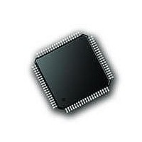
PIC18F87J72-I/PT Microchip Technology, PIC18F87J72-I/PT Datasheet - Page 328

PIC18F87J72-I/PT
Manufacturer Part Number
PIC18F87J72-I/PT
Description
IC PIC MCU 8BIT 14KB FLSH 80TQFP
Manufacturer
Microchip Technology
Series
PIC® 18Fr
Datasheet
1.PIC18F86J72-IPT.pdf
(480 pages)
Specifications of PIC18F87J72-I/PT
Program Memory Type
FLASH
Program Memory Size
128KB (64K x 16)
Package / Case
80-TQFP
Core Processor
PIC
Core Size
8-Bit
Speed
48MHz
Connectivity
I²C, LIN, SPI, UART/USART
Peripherals
Brown-out Detect/Reset, LCD, LVD, POR, PWM, WDT
Number Of I /o
51
Ram Size
3.8K x 8
Voltage - Supply (vcc/vdd)
2 V ~ 3.6 V
Data Converters
A/D 12x12b
Oscillator Type
Internal
Operating Temperature
-40°C ~ 85°C
Data Bus Width
8 bit
Data Ram Size
4 KB
Interface Type
SPI, USART, SPI, I2C
Maximum Clock Frequency
8 MHz
Number Of Programmable I/os
51
Number Of Timers
4
Operating Supply Voltage
2 V to 3.6 V
Maximum Operating Temperature
+ 85 C
Mounting Style
SMD/SMT
Minimum Operating Temperature
- 40 C
On-chip Adc
14
Controller Family/series
PIC18F
No. Of I/o's
51
Ram Memory Size
3923Byte
Cpu Speed
48MHz
No. Of Timers
4
Rohs Compliant
Yes
Lead Free Status / RoHS Status
Lead free / RoHS Compliant
Lead Free Status / RoHS Status
Lead free / RoHS Compliant, Lead free / RoHS Compliant
Available stocks
Company
Part Number
Manufacturer
Quantity
Price
Company:
Part Number:
PIC18F87J72-I/PT
Manufacturer:
Microchip
Quantity:
210
Company:
Part Number:
PIC18F87J72-I/PT
Manufacturer:
Microchip Technology
Quantity:
10 000
- Current page: 328 of 480
- Download datasheet (5Mb)
PIC18F87J72 FAMILY
26.3.2
When the on-chip regulator is enabled, PIC18F87J72
family devices also have a simple Brown-out Reset
capability. If the voltage supplied to the regulator falls to
a level that is inadequate to maintain a regulated output
for full-speed operation, the regulator Reset circuitry
will generate a Brown-out Reset. This event is captured
by the BOR flag bit (RCON<0>).
The operation of the BOR is described in more detail in
Section 5.4
Section 5.4.1 “Detecting BOR”.
26.3.3
The on-chip regulator is designed to meet the power-up
requirements for the device. If the application does not
use the regulator, then strict power-up conditions must
be adhered to. While powering up, V
never exceed V
26.3.4
When enabled, the on-chip regulator always consumes
a small incremental amount of current over I
includes when the device is in Sleep mode, even
though the core digital logic does not require power. To
provide additional savings in applications where power
resources are critical, the regulator can be configured
to automatically disable itself whenever the device
goes into Sleep mode. This feature is controlled by the
REGSLP bit (WDTCON<7>). Setting this bit disables
the regulator in Sleep mode and reduces its current
consumption to a minimum.
Substantial Sleep mode power savings can be
obtained by setting the REGSLP bit, but device
wake-up time will increase in order to ensure the
regulator has enough time to stabilize.
FIGURE 26-3:
DS39979A-page 328
ON-CHIP REGULATOR AND BOR
POWER-UP REQUIREMENTS
OPERATION IN SLEEP MODE
Note 1:
CPU Clock
PLL Clock
Peripheral
Program
Counter
“Brown-out
DD
INTRC
Output
OSC1
Clock
by 0.3 volts.
T
Wake from Interrupt Event
OST
TIMING TRANSITION FOR TWO-SPEED START-UP (INTRC TO HSPLL)
= 1024 T
PC
Reset
OSC
; T
Q1
PLL
T
OST
= 2 ms (approx). These intervals are not shown to scale.
(BOR)”
DDCORE
(1)
Q2
PC + 2
DD
. This
must
T
OSTS bit Set
and
Preliminary
Q3
PLL
(1)
Q4
The REGSLP bit is automatically cleared by hardware
when a Low-Voltage Detect condition occurs. The
REGSLP bit can be set again in software, which would
continue to keep the voltage regulator in Low-Power
mode. This, however, is not recommended if any write
operations to the Flash will be performed.
26.4
The Two-Speed Start-up feature helps to minimize the
latency period, from oscillator start-up to code execu-
tion, by allowing the microcontroller to use the INTRC
oscillator as a clock source until the primary clock
source is available. It is enabled by setting the IESO
Configuration bit.
Two-Speed Start-up should be enabled only if the
primary
(Crystal-Based) modes. Since the EC and ECPLL
modes do not require an OST start-up delay,
Two-Speed Start-up should be disabled.
When enabled, Resets and wake-ups from Sleep mode
cause the device to configure itself to run from the inter-
nal oscillator block as the clock source, following the
time-out of the Power-up Timer after a Power-on Reset
is enabled. This allows almost immediate code
execution while the primary oscillator starts and the
OST is running. Once the OST times out, the device
automatically switches to PRI_RUN mode.
In all other power-managed modes, Two-Speed
Start-up is not used. The device will be clocked by the
currently selected clock source until the primary clock
source becomes available. The setting of the IESO bit
is ignored.
Q1
1
Transition
2
Clock
Two-Speed Start-up
n-1 n
oscillator
PC + 4
Q2
mode
2010 Microchip Technology Inc.
Q3 Q4
is
Q1
PC + 6
HS
Q2
Q3
or
HSPLL
Related parts for PIC18F87J72-I/PT
Image
Part Number
Description
Manufacturer
Datasheet
Request
R

Part Number:
Description:
Manufacturer:
Microchip Technology Inc.
Datasheet:

Part Number:
Description:
Manufacturer:
Microchip Technology Inc.
Datasheet:

Part Number:
Description:
Manufacturer:
Microchip Technology Inc.
Datasheet:

Part Number:
Description:
Manufacturer:
Microchip Technology Inc.
Datasheet:

Part Number:
Description:
Manufacturer:
Microchip Technology Inc.
Datasheet:

Part Number:
Description:
Manufacturer:
Microchip Technology Inc.
Datasheet:

Part Number:
Description:
Manufacturer:
Microchip Technology Inc.
Datasheet:

Part Number:
Description:
Manufacturer:
Microchip Technology Inc.
Datasheet:


