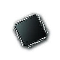
PIC18F87J72-I/PT Microchip Technology, PIC18F87J72-I/PT Datasheet - Page 280

PIC18F87J72-I/PT
Manufacturer Part Number
PIC18F87J72-I/PT
Description
IC PIC MCU 8BIT 14KB FLSH 80TQFP
Manufacturer
Microchip Technology
Series
PIC® 18Fr
Datasheet
1.PIC18F86J72-IPT.pdf
(480 pages)
Specifications of PIC18F87J72-I/PT
Program Memory Type
FLASH
Program Memory Size
128KB (64K x 16)
Package / Case
80-TQFP
Core Processor
PIC
Core Size
8-Bit
Speed
48MHz
Connectivity
I²C, LIN, SPI, UART/USART
Peripherals
Brown-out Detect/Reset, LCD, LVD, POR, PWM, WDT
Number Of I /o
51
Ram Size
3.8K x 8
Voltage - Supply (vcc/vdd)
2 V ~ 3.6 V
Data Converters
A/D 12x12b
Oscillator Type
Internal
Operating Temperature
-40°C ~ 85°C
Data Bus Width
8 bit
Data Ram Size
4 KB
Interface Type
SPI, USART, SPI, I2C
Maximum Clock Frequency
8 MHz
Number Of Programmable I/os
51
Number Of Timers
4
Operating Supply Voltage
2 V to 3.6 V
Maximum Operating Temperature
+ 85 C
Mounting Style
SMD/SMT
Minimum Operating Temperature
- 40 C
On-chip Adc
14
Controller Family/series
PIC18F
No. Of I/o's
51
Ram Memory Size
3923Byte
Cpu Speed
48MHz
No. Of Timers
4
Rohs Compliant
Yes
Lead Free Status / RoHS Status
Lead free / RoHS Compliant
Lead Free Status / RoHS Status
Lead free / RoHS Compliant, Lead free / RoHS Compliant
Available stocks
Company
Part Number
Manufacturer
Quantity
Price
Company:
Part Number:
PIC18F87J72-I/PT
Manufacturer:
Microchip
Quantity:
210
Company:
Part Number:
PIC18F87J72-I/PT
Manufacturer:
Microchip Technology
Quantity:
10 000
- Current page: 280 of 480
- Download datasheet (5Mb)
conversion sample. This means the ADRESH:ADRESL
PIC18F87J72 FAMILY
21.5
Figure 21-1 shows the operation of the A/D Converter
after the GO/DONE bit has been set and the
ACQT<2:0> bits are cleared. A conversion is started
after the following instruction to allow entry into Sleep
mode before the conversion begins.
Figure 21-2 shows the operation of the A/D Converter
after the GO/DONE bit has been set. The ACQT<2:0>
bits are set to ‘010’ and a 4 T
selected before the conversion starts.
Clearing the GO/DONE bit during a conversion will abort
the current conversion. The A/D Result register pair will
NOT be updated with the partially completed A/D
registers will continue to contain the value of the last
completed conversion (or the last value written to the
ADRESH:ADRESL registers).
After the A/D conversion is completed or aborted, a
2 T
be started. After this wait, acquisition on the selected
channel is automatically started.
FIGURE 21-1:
FIGURE 21-2:
DS39979A-page 280
(Holding capacitor continues
acquiring input)
Note:
Set GO/DONE bit
T
AD
Set GO/DONE bit
CY
Holding capacitor is disconnected from analog input (typically 100 ns)
1
wait is required before the next acquisition can
– T
T
ACQT
A/D Conversions
Acquisition
AD
Automatic
2
The GO/DONE bit should NOT be set in
the same instruction that turns on the A/D.
Time
T
AD
Cycles
1 T
3
Conversion starts
b11
AD
A/D CONVERSION T
A/D CONVERSION T
2 T
4
AD
b10
1
3 T
Conversion starts
(Holding capacitor is disconnected)
AD
AD
b11
b9
2
acquisition time is
4 T
b10
On the following cycle:
ADRESH:ADRESL are loaded, GO/DONE bit is cleared,
ADIF bit is set, holding capacitor is connected to analog input
AD
3
b8
5 T
On the following cycle:
ADRESH:ADRESL are loaded, GO/DONE bit is cleared,
ADIF bit is set, holding capacitor is connected to analog input
AD
AD
b9
AD
4
b7
6 T
CYCLES (ACQT<2:0> = 000, T
CYCLES (ACQT<2:0> = 010, T
Preliminary
5
b8
AD
b6
7 T
T
b7
6
AD
AD
b5
8
Cycles
21.6
An A/D conversion can be started by the “Special Event
Trigger” of the CCP2 module. This requires that the
CCP2M<3:0> bits (CCP2CON<3:0>) be programmed
as ‘1011’ and that the A/D module is enabled (ADON
bit is set). When the trigger occurs, the GO/DONE bit
will be set, starting the A/D acquisition and conversion,
and the Timer1 (or Timer3) counter will be reset to zero.
Timer1 (or Timer3) is reset to automatically repeat the
A/D acquisition period with minimal software overhead
(moving ADRESH:ADRESL to the desired location).
The appropriate analog input channel must be selected
and the minimum acquisition period is either timed by
the user or an appropriate T
the Special Event Trigger sets the GO/DONE bit (starts
a conversion).
If the A/D module is not enabled (ADON is cleared), the
Special Event Trigger will be ignored by the A/D module,
but will still reset the Timer1 (or Timer3) counter.
b6
7
T
AD
b4
9 T
b5
8
Use of the CCP2 Trigger
AD
b3
10
b4
9
T
AD
b2
11
b3
10
ACQ
T
ACQ
AD
2010 Microchip Technology Inc.
b1
11
b2
12
ACQ
= 0)
= 4 T
T
AD
b0
12
time is selected before
b1
13
AD
)
T
Discharge
(typically 200 ns)
b0
AD
13
1
T
Discharge
(typically
200 ns)
AD
1
Related parts for PIC18F87J72-I/PT
Image
Part Number
Description
Manufacturer
Datasheet
Request
R

Part Number:
Description:
Manufacturer:
Microchip Technology Inc.
Datasheet:

Part Number:
Description:
Manufacturer:
Microchip Technology Inc.
Datasheet:

Part Number:
Description:
Manufacturer:
Microchip Technology Inc.
Datasheet:

Part Number:
Description:
Manufacturer:
Microchip Technology Inc.
Datasheet:

Part Number:
Description:
Manufacturer:
Microchip Technology Inc.
Datasheet:

Part Number:
Description:
Manufacturer:
Microchip Technology Inc.
Datasheet:

Part Number:
Description:
Manufacturer:
Microchip Technology Inc.
Datasheet:

Part Number:
Description:
Manufacturer:
Microchip Technology Inc.
Datasheet:


