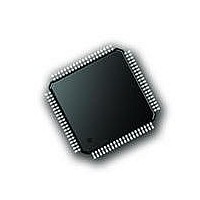
PIC18F87J72-I/PT Microchip Technology, PIC18F87J72-I/PT Datasheet - Page 453

PIC18F87J72-I/PT
Manufacturer Part Number
PIC18F87J72-I/PT
Description
IC PIC MCU 8BIT 14KB FLSH 80TQFP
Manufacturer
Microchip Technology
Series
PIC® 18Fr
Datasheet
1.PIC18F86J72-IPT.pdf
(480 pages)
Specifications of PIC18F87J72-I/PT
Program Memory Type
FLASH
Program Memory Size
128KB (64K x 16)
Package / Case
80-TQFP
Core Processor
PIC
Core Size
8-Bit
Speed
48MHz
Connectivity
I²C, LIN, SPI, UART/USART
Peripherals
Brown-out Detect/Reset, LCD, LVD, POR, PWM, WDT
Number Of I /o
51
Ram Size
3.8K x 8
Voltage - Supply (vcc/vdd)
2 V ~ 3.6 V
Data Converters
A/D 12x12b
Oscillator Type
Internal
Operating Temperature
-40°C ~ 85°C
Data Bus Width
8 bit
Data Ram Size
4 KB
Interface Type
SPI, USART, SPI, I2C
Maximum Clock Frequency
8 MHz
Number Of Programmable I/os
51
Number Of Timers
4
Operating Supply Voltage
2 V to 3.6 V
Maximum Operating Temperature
+ 85 C
Mounting Style
SMD/SMT
Minimum Operating Temperature
- 40 C
On-chip Adc
14
Controller Family/series
PIC18F
No. Of I/o's
51
Ram Memory Size
3923Byte
Cpu Speed
48MHz
No. Of Timers
4
Rohs Compliant
Yes
Lead Free Status / RoHS Status
Lead free / RoHS Compliant
Lead Free Status / RoHS Status
Lead free / RoHS Compliant, Lead free / RoHS Compliant
Available stocks
Company
Part Number
Manufacturer
Quantity
Price
Company:
Part Number:
PIC18F87J72-I/PT
Manufacturer:
Microchip
Quantity:
210
Company:
Part Number:
PIC18F87J72-I/PT
Manufacturer:
Microchip Technology
Quantity:
10 000
- Current page: 453 of 480
- Download datasheet (5Mb)
B.5.7.1
Both ADCs are powered up with their default
configurations and begin to output DR pulses
immediately (RESET<1:0> and SHUTDOWN<1:0>
bits are all ‘0’ by default).
The default output codes for both ADCs are all zeros.
The default modulator output for both ADCs is ‘0011’
(corresponding to a theoretical zero voltage at the
inputs). The default phase is zero between the two
channels.
It is recommended to enter into ADC Reset mode for
both ADCs just after power-up because the desired
register configuration may not be the default one, and
in this case, the ADC would output undesired data.
Within the ADC Reset mode (RESET<1:0> = 11), the
user can configure the whole part with a single commu-
nication. The write commands increment the address
automatically so that the user can start writing the
PHASE register, and finish with the CONFIG2 register,
in only one communication (see Figure B-11). The
RESET<1:0> bits are in the CONFIG2 register to allow
exiting of the Soft Reset mode, and have the whole part
configured and ready to run in only one command.
The following register sets are defined as groups:
TABLE B-11:
FIGURE B-12: RECOMMENDED CONFIGURATION SEQUENCE AT POWER UP
2010 Microchip Technology Inc.
ADC DATA CH0
ADC DATA CH1
PHASE, GAIN
CONFIG, STATUS
AV
CS
SCK
SDI
DD
GROUP
CONFIG2 ADDR/W
Optional Reset of Both ADCs
Continuous Write
00011000
REGISTER GROUPS
11XXXXX1
CONFIG2
ADDRESSES
0x09-0x0B
0x00-0x02
0x03-0x05
0x07-0x08
PHASE ADDR/W
00001110
Preliminary
xxxxxxxx
PHASE
One Command for Writing Complete Configuration
PIC18F87J72 FAMILY
The following register sets are defined as types:
TABLE B-12:
B.5.8
Immediately after the following actions, the ADCs are
temporarily reset in order to provide proper operation:
1.
2.
3.
4.
5.
After these temporary Resets, the ADCs go back to the
normal operation with no need for an additional
command. These are also the settings where the DR
position is affected. The PHASE register can be used
to serially soft reset the ADCs without using the RESET
bits in the Configuration register if the same value is
written in the PHASE register.
ADC DATA
(Both Channels)
CONFIGURATION
xxxxxxxx
Change in the PHASE register.
Change in the OSR setting.
Change in the PRESCALE setting.
Overwrite of the same PHASE register value.
Change in the CLKEXT bit in the CONFIG2
register, modifying the internal oscillator state.
GAIN
TYPE
SITUATIONS THAT RESET ADC
DATA
STATUS/COM
xxxxxxxx
REGISTER TYPES
xxxxxxxx
CONFIG1
ADDRESSES
0x07-0x0B
0x00-x05
DS39979A-page 453
xxxxxxxx
CONFIG2
Related parts for PIC18F87J72-I/PT
Image
Part Number
Description
Manufacturer
Datasheet
Request
R

Part Number:
Description:
Manufacturer:
Microchip Technology Inc.
Datasheet:

Part Number:
Description:
Manufacturer:
Microchip Technology Inc.
Datasheet:

Part Number:
Description:
Manufacturer:
Microchip Technology Inc.
Datasheet:

Part Number:
Description:
Manufacturer:
Microchip Technology Inc.
Datasheet:

Part Number:
Description:
Manufacturer:
Microchip Technology Inc.
Datasheet:

Part Number:
Description:
Manufacturer:
Microchip Technology Inc.
Datasheet:

Part Number:
Description:
Manufacturer:
Microchip Technology Inc.
Datasheet:

Part Number:
Description:
Manufacturer:
Microchip Technology Inc.
Datasheet:


