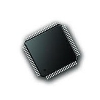
PIC18F87J72-I/PT Microchip Technology, PIC18F87J72-I/PT Datasheet - Page 460

PIC18F87J72-I/PT
Manufacturer Part Number
PIC18F87J72-I/PT
Description
IC PIC MCU 8BIT 14KB FLSH 80TQFP
Manufacturer
Microchip Technology
Series
PIC® 18Fr
Datasheet
1.PIC18F86J72-IPT.pdf
(480 pages)
Specifications of PIC18F87J72-I/PT
Program Memory Type
FLASH
Program Memory Size
128KB (64K x 16)
Package / Case
80-TQFP
Core Processor
PIC
Core Size
8-Bit
Speed
48MHz
Connectivity
I²C, LIN, SPI, UART/USART
Peripherals
Brown-out Detect/Reset, LCD, LVD, POR, PWM, WDT
Number Of I /o
51
Ram Size
3.8K x 8
Voltage - Supply (vcc/vdd)
2 V ~ 3.6 V
Data Converters
A/D 12x12b
Oscillator Type
Internal
Operating Temperature
-40°C ~ 85°C
Data Bus Width
8 bit
Data Ram Size
4 KB
Interface Type
SPI, USART, SPI, I2C
Maximum Clock Frequency
8 MHz
Number Of Programmable I/os
51
Number Of Timers
4
Operating Supply Voltage
2 V to 3.6 V
Maximum Operating Temperature
+ 85 C
Mounting Style
SMD/SMT
Minimum Operating Temperature
- 40 C
On-chip Adc
14
Controller Family/series
PIC18F
No. Of I/o's
51
Ram Memory Size
3923Byte
Cpu Speed
48MHz
No. Of Timers
4
Rohs Compliant
Yes
Lead Free Status / RoHS Status
Lead free / RoHS Compliant
Lead Free Status / RoHS Status
Lead free / RoHS Compliant, Lead free / RoHS Compliant
Available stocks
Company
Part Number
Manufacturer
Quantity
Price
Company:
Part Number:
PIC18F87J72-I/PT
Manufacturer:
Microchip
Quantity:
210
Company:
Part Number:
PIC18F87J72-I/PT
Manufacturer:
Microchip Technology
Quantity:
10 000
- Current page: 460 of 480
- Download datasheet (5Mb)
PIC18F87J72 FAMILY
B.6.4
This register contains all settings related to the
communication, including data ready settings and
status, and Read mode settings.
B.6.4.1
This bit determines if the first data ready pulses
correspond to settled data, or unsettled data, from each
SINC
every DRCLK period. If this bit is set, unsettled data will
wait for 3 DRCLK periods before giving DR pulses and
will then give DR pulses every DRCLK period.
B.6.4.2
This bit defines the non-active state of the Data Ready
pin (logic ‘1’ or high-impedance). Using this bit, the
user can connect multiple chips with the same DR pin
with a pull-up resistor (DR_HIZN = 0) or a single chip
with no external component (DR_HIZN = 1).
B.6.4.3
If one of the channels is in Reset or shutdown, only one
of the data ready pulses is present and the situation is
similar to DRMODE = 01 or 10. In the ‘01’, ‘10’ and ‘11’
modes, the ADC channel data to be read is latched at
the beginning of a reading, in order to prevent the case
of erroneous data when a DR pulse happens during a
read. In these modes the two channels are independent.
When these bits are equal to ‘11’, ‘10’ or ‘01’, they con-
trol which ADC’s data ready is present on the DR pin.
When DRMODE = 00, the Data Ready pin output is
synchronized with the lagging ADC channel (defined by
the PHASE register) and the ADCs are linked together.
In this mode, the output of the two ADCs are latched
synchronously at the moment of the DR event. This
prevents having bad synchronization between the two
ADCs. The output is also latched at the beginning of a
reading in order not to be updated during a read and
not to give erroneous data.
DS39979A-page 460
3
filter. Unsettled data will provide DR pulses
STATUS AND COMMUNICATION
REGISTER
Data Ready (DR) Latency Control –
DR_LTY
Data Ready (DR) Pin High-Z –
DR_HIZN
Data Ready Mode – DRMODE<1:0>
Preliminary
This mode is very useful for power metering
applications because the data from both ADCs can be
retrieved using this single data ready event which is
processed synchronously, even in case of a large
phase difference. This mode works as if there was one
ADC channel and its data would be 48 bits long, and
contain both channel data. As a consequence, if one
channel is in Reset or shutdown when DRMODE = 00,
no data ready pulse will be present at the outputs (if
both channels are not ready in this mode, the data is
not considered as ready).
See Section B.5.9 “Data Ready Pin (DR)” for more
details about Data Ready pin behavior.
B.6.4.4
These bits indicate the DR status of both channels,
respectively. These flags are set to logic high after each
read of the STATUS/COM register. These bits are
cleared when a DR event has happened on its
respective ADC channel. Writing these bits has no
effect.
Note:
These bits are useful if multiple devices
share
(DR_HIZN = 0) in order to understand
from which device the DR event has
happened. This configuration can be used
for three-phase power metering systems
where all three phases share the same
Data Ready pin. In case the DRMODE = 00
(linked ADCs), these data ready status bits
will be updated synchronously upon the
same event (lagging ADC is ready). These
bits are also useful in systems where the
DR pin is not used to save MCU I/O.
DR Status Flag – DRSTATUS<1:0>
the
2010 Microchip Technology Inc.
same
DR
output
pin
Related parts for PIC18F87J72-I/PT
Image
Part Number
Description
Manufacturer
Datasheet
Request
R

Part Number:
Description:
Manufacturer:
Microchip Technology Inc.
Datasheet:

Part Number:
Description:
Manufacturer:
Microchip Technology Inc.
Datasheet:

Part Number:
Description:
Manufacturer:
Microchip Technology Inc.
Datasheet:

Part Number:
Description:
Manufacturer:
Microchip Technology Inc.
Datasheet:

Part Number:
Description:
Manufacturer:
Microchip Technology Inc.
Datasheet:

Part Number:
Description:
Manufacturer:
Microchip Technology Inc.
Datasheet:

Part Number:
Description:
Manufacturer:
Microchip Technology Inc.
Datasheet:

Part Number:
Description:
Manufacturer:
Microchip Technology Inc.
Datasheet:


