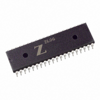
Z85C3010PSG Zilog, Z85C3010PSG Datasheet - Page 161

Z85C3010PSG
Manufacturer Part Number
Z85C3010PSG
Description
IC 10MHZ Z8500 CMOS SCC 40-DIP
Manufacturer
Zilog
Series
SCCr
Specifications of Z85C3010PSG
Processor Type
Z80
Features
Error Detection and Multiprotocol Support
Speed
10MHz
Voltage
5V
Mounting Type
Through Hole
Package / Case
40-DIP (0.620", 15.75mm)
Cpu Speed
8MHz
Digital Ic Case Style
DIP
No. Of Pins
40
Supply Voltage Range
5V
Operating Temperature Range
0°C To +70°C
Svhc
No SVHC (18-Jun-2010)
Base Number
85
Rohs Compliant
Yes
Clock Frequency
10MHz
Lead Free Status / RoHS Status
Lead free / RoHS Compliant
Other names
269-3934
Z85C3010PSG
Z85C3010PSG
Available stocks
Company
Part Number
Manufacturer
Quantity
Price
Company:
Part Number:
Z85C3010PSG
Manufacturer:
Zilog
Quantity:
135
Company:
Part Number:
Z85C3010PSG
Manufacturer:
Zilog
Quantity:
326
- Current page: 161 of 317
- Download datasheet (4Mb)
Application Note
The Z180™ Interfaced with the SCC at MHZ
INTERFACES
The following subsections explain the interfaces between
the:
Basic goals of this system design are:
6-26
Z180 and Memory
Z180 and I/O
Z180 and SCC
System clock up to 10 MHz
Using the Z8018010VSC (Z180 10 MHz PLCC
package) to take advantage of 1M byte addressing
space and compactness (DIP versions’ addressing
range is half; 512K bytes)
Using Z85C3010VSC (CMOS SCC 10 MHz PLCC
package)
Minimum parts count
Worst case design
Address
/MREQ
Data
/RD
/M1
Ø
Figure 1. Z180 Opcode Fetch Cycle Timing (One Wait State)
T1
6
10
8
9
T2
7
The design method for EPLD is using TTLs (74HCT) and
then translating them into EPLD logic. This design uses
TTLs and EPLDs. With these goals in mind, the discussion
begins with the Z180-to-memory interface.
Z180 to Memory Interface
The memory access cycle timing of the Z180 is similar to
the Z80 CPU memory access cycle timing. The three
classifications are:
Table 1 shows the Z180’s basic timing elements for the
opcode’s fetch/memory read/write cycle.
Tw
Using EPLD for glue wherever possible
Expendability
Opcode fetch cycle (Figure 1)
Memory read cycle (Figure 2)
Memory write cycle (Figure 3)
Read Data
T3
14
15
12
13
T1
11
11
16
UM010901-0601
Related parts for Z85C3010PSG
Image
Part Number
Description
Manufacturer
Datasheet
Request
R

Part Number:
Description:
Manufacturer:
Zilog, Inc.
Datasheet:

Part Number:
Description:
Cmos Scc Serial Communications Controller
Manufacturer:
ZiLOG Semiconductor
Datasheet:

Part Number:
Description:
Communication Controllers, ZILOG INTELLIGENT PERIPHERAL CONTROLLER (ZIP)
Manufacturer:
Zilog, Inc.
Datasheet:

Part Number:
Description:
KIT DEV FOR Z8 ENCORE 16K TO 64K
Manufacturer:
Zilog
Datasheet:

Part Number:
Description:
KIT DEV Z8 ENCORE XP 28-PIN
Manufacturer:
Zilog
Datasheet:

Part Number:
Description:
DEV KIT FOR Z8 ENCORE 8K/4K
Manufacturer:
Zilog
Datasheet:

Part Number:
Description:
KIT DEV Z8 ENCORE XP 28-PIN
Manufacturer:
Zilog
Datasheet:

Part Number:
Description:
DEV KIT FOR Z8 ENCORE 4K TO 8K
Manufacturer:
Zilog
Datasheet:

Part Number:
Description:
CMOS Z8 microcontroller. ROM 16 Kbytes, RAM 256 bytes, speed 16 MHz, 32 lines I/O, 3.0V to 5.5V
Manufacturer:
Zilog, Inc.
Datasheet:

Part Number:
Description:
Low-cost microcontroller. 512 bytes ROM, 61 bytes RAM, 8 MHz
Manufacturer:
Zilog, Inc.
Datasheet:

Part Number:
Description:
Z8 4K OTP Microcontroller
Manufacturer:
Zilog, Inc.
Datasheet:

Part Number:
Description:
CMOS SUPER8 ROMLESS MCU
Manufacturer:
Zilog, Inc.
Datasheet:

Part Number:
Description:
SL1866 CMOSZ8 OTP Microcontroller
Manufacturer:
Zilog, Inc.
Datasheet:


