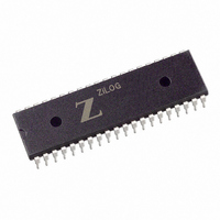
Z85C3010PSG Zilog, Z85C3010PSG Datasheet - Page 30

Z85C3010PSG
Manufacturer Part Number
Z85C3010PSG
Description
IC 10MHZ Z8500 CMOS SCC 40-DIP
Manufacturer
Zilog
Series
SCCr
Specifications of Z85C3010PSG
Processor Type
Z80
Features
Error Detection and Multiprotocol Support
Speed
10MHz
Voltage
5V
Mounting Type
Through Hole
Package / Case
40-DIP (0.620", 15.75mm)
Cpu Speed
8MHz
Digital Ic Case Style
DIP
No. Of Pins
40
Supply Voltage Range
5V
Operating Temperature Range
0°C To +70°C
Svhc
No SVHC (18-Jun-2010)
Base Number
85
Rohs Compliant
Yes
Clock Frequency
10MHz
Lead Free Status / RoHS Status
Lead free / RoHS Compliant
Other names
269-3934
Z85C3010PSG
Z85C3010PSG
Available stocks
Company
Part Number
Manufacturer
Quantity
Price
Company:
Part Number:
Z85C3010PSG
Manufacturer:
Zilog
Quantity:
135
Company:
Part Number:
Z85C3010PSG
Manufacturer:
Zilog
Quantity:
326
- Current page: 30 of 317
- Download datasheet (4Mb)
UM010901-0601
2.3.2 Z85X30 Write Cycle Timing
The write cycle timing for the Z85X30 is shown in Figure 2-
6. The address on A//B and D//C, as well as the data on
D7-D0, is latched by the coincidence of /WR and /CE ac-
tive. /CE must remain Low and /INTACK must remain High
throughout the cycle. A write cycle with D//C High does not
disturb the state of the pointers and a write cycle with D//C
Low resets the pointers to zero after the internal operation
is complete.
2.3.3 Z85X30 Interrupt Acknowledge Cycle Timing
The interrupt acknowledge cycle timing for the Z85X30 is
shown in Figure 2-7. The state of /INTACK is latched by
A//B, D//C
/INTACK
/INTACK
D7-D0
D7-D0
/CE
/WR
/RD
Note: Dotted line is ESCC only.
Figure 2-7. Z85X30 Interrupt Acknowledge Cycle Timing
Figure 2-6. Z85X30 Write Cycle Timing
See Note
Historically, the NMOS/CMOS version latched the data
bus on the falling edge of /WR. However, many CPUs do
not guarantee that the data bus is valid at the time when
the /WR pin goes low, so the data bus timing was modified
to allow a maximum delay from the falling edge of /WR to
the latching of the data bus. On the Z85230, the AC Timing
parameter #29 TsDW(WR), Write Data to /WR falling min-
imum, has been changed to: /WR falling to Write Data Val-
id maximum. Refer to the AC Timing Characteristic section
of the Z85230 Product Specification for more information
regarding this change.
the rising edge of PCLK (AC Spec #10). While /INTACK is
Low, the state of A//B, /CE, D//C, and /WR are ignored.
Address Valid
Data Valid
Vector
SCC™/ESCC™ User’s Manual
Interfacing the SCC/ESCC
2-11
2
Related parts for Z85C3010PSG
Image
Part Number
Description
Manufacturer
Datasheet
Request
R

Part Number:
Description:
Manufacturer:
Zilog, Inc.
Datasheet:

Part Number:
Description:
Cmos Scc Serial Communications Controller
Manufacturer:
ZiLOG Semiconductor
Datasheet:

Part Number:
Description:
Communication Controllers, ZILOG INTELLIGENT PERIPHERAL CONTROLLER (ZIP)
Manufacturer:
Zilog, Inc.
Datasheet:

Part Number:
Description:
KIT DEV FOR Z8 ENCORE 16K TO 64K
Manufacturer:
Zilog
Datasheet:

Part Number:
Description:
KIT DEV Z8 ENCORE XP 28-PIN
Manufacturer:
Zilog
Datasheet:

Part Number:
Description:
DEV KIT FOR Z8 ENCORE 8K/4K
Manufacturer:
Zilog
Datasheet:

Part Number:
Description:
KIT DEV Z8 ENCORE XP 28-PIN
Manufacturer:
Zilog
Datasheet:

Part Number:
Description:
DEV KIT FOR Z8 ENCORE 4K TO 8K
Manufacturer:
Zilog
Datasheet:

Part Number:
Description:
CMOS Z8 microcontroller. ROM 16 Kbytes, RAM 256 bytes, speed 16 MHz, 32 lines I/O, 3.0V to 5.5V
Manufacturer:
Zilog, Inc.
Datasheet:

Part Number:
Description:
Low-cost microcontroller. 512 bytes ROM, 61 bytes RAM, 8 MHz
Manufacturer:
Zilog, Inc.
Datasheet:

Part Number:
Description:
Z8 4K OTP Microcontroller
Manufacturer:
Zilog, Inc.
Datasheet:

Part Number:
Description:
CMOS SUPER8 ROMLESS MCU
Manufacturer:
Zilog, Inc.
Datasheet:

Part Number:
Description:
SL1866 CMOSZ8 OTP Microcontroller
Manufacturer:
Zilog, Inc.
Datasheet:


