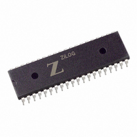
Z85C3010PSG Zilog, Z85C3010PSG Datasheet - Page 299

Z85C3010PSG
Manufacturer Part Number
Z85C3010PSG
Description
IC 10MHZ Z8500 CMOS SCC 40-DIP
Manufacturer
Zilog
Series
SCCr
Specifications of Z85C3010PSG
Processor Type
Z80
Features
Error Detection and Multiprotocol Support
Speed
10MHz
Voltage
5V
Mounting Type
Through Hole
Package / Case
40-DIP (0.620", 15.75mm)
Cpu Speed
8MHz
Digital Ic Case Style
DIP
No. Of Pins
40
Supply Voltage Range
5V
Operating Temperature Range
0°C To +70°C
Svhc
No SVHC (18-Jun-2010)
Base Number
85
Rohs Compliant
Yes
Clock Frequency
10MHz
Lead Free Status / RoHS Status
Lead free / RoHS Compliant
Other names
269-3934
Z85C3010PSG
Z85C3010PSG
Available stocks
Company
Part Number
Manufacturer
Quantity
Price
Company:
Part Number:
Z85C3010PSG
Manufacturer:
Zilog
Quantity:
135
Company:
Part Number:
Z85C3010PSG
Manufacturer:
Zilog
Quantity:
326
- Current page: 299 of 317
- Download datasheet (4Mb)
Application Note
Interfacing the ISCC™ to the 68000 and 8086
determines which byte of the bus data is accepted. The
byte swapping feature activates by programming the Byte
Swap Enable bit to a 1 in the BCR. The odd/even byte
transfer selection occurs by programming the Byte Swap
Select bit in the BCR. If Byte Swap Select is a 1, then even
address bytes (transfers where the DMA address has A0
= 0) are accepted on the lower 8 bits of the bus. Odd
address bytes (transfers where the DMA address has A0
= 1) are accepted on the upper 8 bits of the bus. If Byte
Swap Select is a 0, then even address bytes (transfers
where the DMA address has A0 = 0) are accepted on the
upper 8 bits of the bus. Odd address bytes (transfers
where the DMA address has A0 =1) are accepted on the
lower 8 bits of the bus.
Bus Interface Handshaking
The ISCC™ supports data transfers by either a data strobe
(DS) combined with a read/write (R/W) status line, or
separate read (RD) and write (WR) strobes. These
transactions activate via chip enable (CE).
ISCC programming generates interrupts upon the
occurrence of certain internal events. The ISCC internally
prioritizes its own interrupts, therefore, the ISCC presents
one interrupt to the processor even though lower priority
internal interrupts may be pending. Interrupts are
individually enabled or disabled. Refer to the sections on
the SCC core.
Interrupt Acknowledge (INTACK) is an input to the ISCC
showing
progressing. INTACK is programmed to accept a status
acknowledge, a single pulse acknowledge, or a double
pulse acknowledge. This programming activates in the
BCR. The double pulse acknowledge is compatible with
8X86 family microprocessors and the status acknowledge
is compatible with 68000 family microprocessors.
During an interrupt acknowledge cycle, the SCC and DMA
interrupt priority daisy chain internally resolves. Thus, the
highest priority internal interrupt is presented to the CPU.
6-4
BUS DATA TRANSFERS (Continued)
that
an
interrupt
acknowledge
cycle
is
The ISCC can return an interrupt vector that encodes with
the type of interrupt pending enabled during this
acknowledge cycle. The ISCC may request an interrupt
but not return an interrupt vector [note that the no vector
bit(s) in the SCC section (WR9 bit 1) and in the DMA
section (ICR bit 5) individually control whether or not an
interrupt vector returns by these cores]. The interrupt
vector can program to include a status field showing the
internal ISCC source of the interrupt. During the interrupt
acknowledge cycle, the ISCC returns the interrupt vector
when INTACK, RD or DS go active and IEI is high (if the
ISCC is not programmed for the no vector option).
During the programmed pulsed acknowledge type
(whether single or double), INTACK is the strobe for the
interrupt vector. Thus when INTACK goes active, the ISCC
drives the bus and presents the interrupt vector to the
CPU. When the status acknowledge type programs, the
ISCC drives the bus with the interrupt vector when RD or
DS are active.
WAITRDY programs to function either as a WAIT signal or
a READY signal using the BCR write. When programmed
as a wait signal, it supports the READY function of 8X86
family microprocessors. When programmed as a ready
signal, it supports the DTACK function of 680x0 family
microprocessors.
The WAIT/RDY signal functions as an output when the
ISCC is not a bus master. In this case, this signal serves
to indicate when the data is available during a read cycle,
when the device is ready to receive data during a write
cycle, and when a valid vector is available during an
interrupt acknowledge cycle.
When the ISCC is the bus master (DMA section has taken
control of the bus), the WAIT/RDY signal functions as a
WAIT or RDY input. Slow memories and peripheral
devices use WAIT to extend the data strobe (/DS) during
bus transfers. Similarly, memories and peripheral devices
use RDY to indicate valid output or that it is ready to latch
input data.
UM010901-0601
Related parts for Z85C3010PSG
Image
Part Number
Description
Manufacturer
Datasheet
Request
R

Part Number:
Description:
Manufacturer:
Zilog, Inc.
Datasheet:

Part Number:
Description:
Cmos Scc Serial Communications Controller
Manufacturer:
ZiLOG Semiconductor
Datasheet:

Part Number:
Description:
Communication Controllers, ZILOG INTELLIGENT PERIPHERAL CONTROLLER (ZIP)
Manufacturer:
Zilog, Inc.
Datasheet:

Part Number:
Description:
KIT DEV FOR Z8 ENCORE 16K TO 64K
Manufacturer:
Zilog
Datasheet:

Part Number:
Description:
KIT DEV Z8 ENCORE XP 28-PIN
Manufacturer:
Zilog
Datasheet:

Part Number:
Description:
DEV KIT FOR Z8 ENCORE 8K/4K
Manufacturer:
Zilog
Datasheet:

Part Number:
Description:
KIT DEV Z8 ENCORE XP 28-PIN
Manufacturer:
Zilog
Datasheet:

Part Number:
Description:
DEV KIT FOR Z8 ENCORE 4K TO 8K
Manufacturer:
Zilog
Datasheet:

Part Number:
Description:
CMOS Z8 microcontroller. ROM 16 Kbytes, RAM 256 bytes, speed 16 MHz, 32 lines I/O, 3.0V to 5.5V
Manufacturer:
Zilog, Inc.
Datasheet:

Part Number:
Description:
Low-cost microcontroller. 512 bytes ROM, 61 bytes RAM, 8 MHz
Manufacturer:
Zilog, Inc.
Datasheet:

Part Number:
Description:
Z8 4K OTP Microcontroller
Manufacturer:
Zilog, Inc.
Datasheet:

Part Number:
Description:
CMOS SUPER8 ROMLESS MCU
Manufacturer:
Zilog, Inc.
Datasheet:

Part Number:
Description:
SL1866 CMOSZ8 OTP Microcontroller
Manufacturer:
Zilog, Inc.
Datasheet:


